
Low Voltage NPN with Low Trigger Voltage and High Snap Back Voltage for ESD Protection

a low-voltage npn and esd protection technology, applied in the field of integrated circuit devices, can solve the problems of difficult practical level solutions for providing a discharge protection circuit which is capable of low triggering voltage (vtb>1/b>) and high snapback voltage (vsb) with minimal circuit footprin

Active Publication Date: 2015-08-20
NXP USA INC
View PDF7 Cites 16 Cited by
  • Summary
  • Abstract
  • Description
  • Claims
  • Application Information

AI Technical Summary

Benefits of technology

The present invention provides a semiconductor device and method for manufacturing the same that uses low voltage NPN bipolar junction transistors for electrostatic discharge (ESD) protection in integrated circuits. The NPN-based ESD protection circuit has a simplified circuit design and is effective in protecting low voltage pins against voltage or current fluctuations. The method for manufacturing the NPN-based ESD protection circuit includes forming halo extension regions around the collector and emitter regions to improve the second trigger or breakdown current. The technical effects of the invention include reducing the footprint of the ESD protection circuits and improving their functionality while maintaining their robustness.

Problems solved by technology

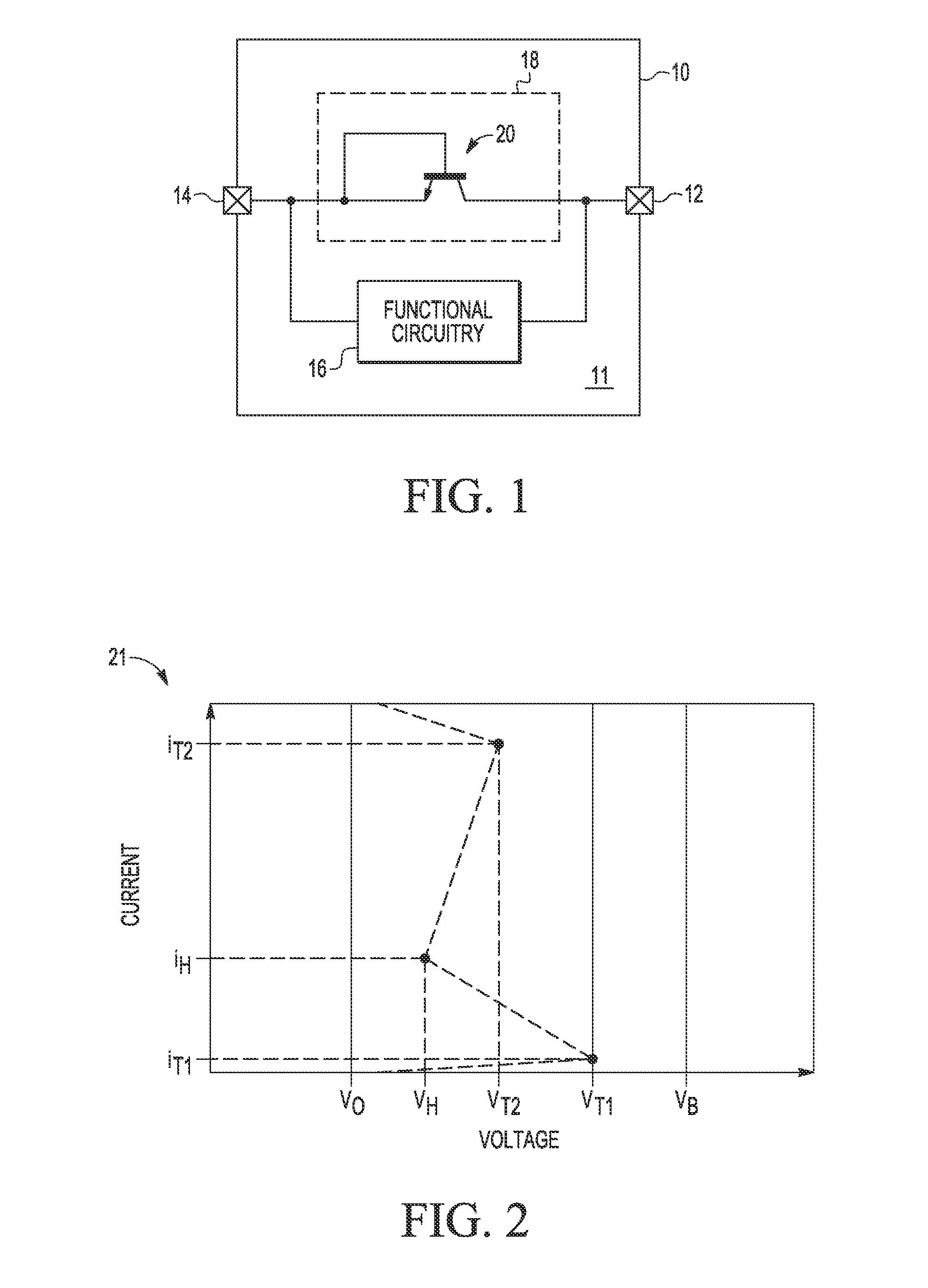
In certain applications for protecting low voltage pins (e.g., 5V-5.5V) against transient current and voltage changes, the existing solutions for providing a discharge protection circuit which is capable of low triggering voltage (Vt1) and high snapback voltage (Vsb) with minimal circuit footprint is extremely difficult at a practical level.

Method used


Image

  • Low Voltage NPN with Low Trigger Voltage and High Snap Back Voltage for ESD Protection
  • Low Voltage NPN with Low Trigger Voltage and High Snap Back Voltage for ESD Protection
  • Low Voltage NPN with Low Trigger Voltage and High Snap Back Voltage for ESD Protection

Examples


Embodiment Construction

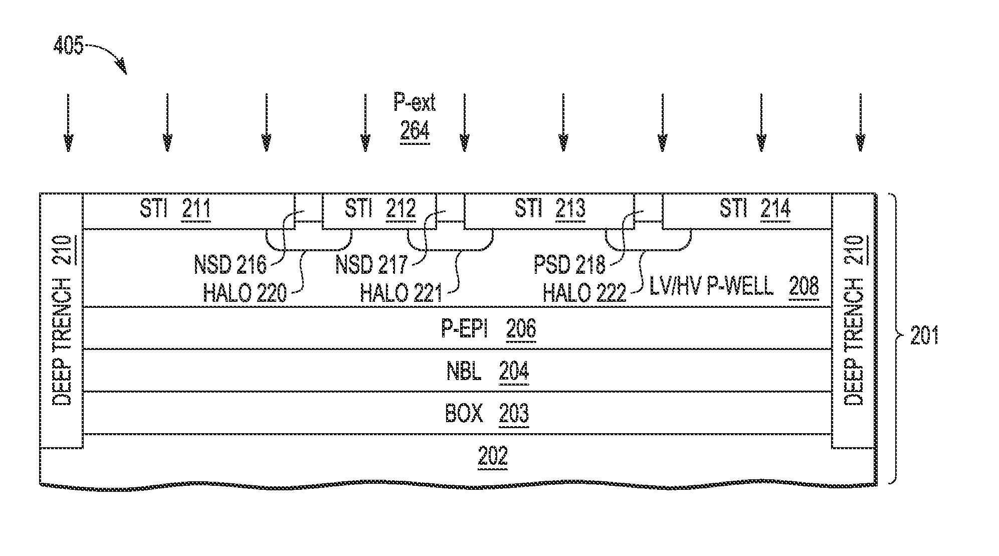
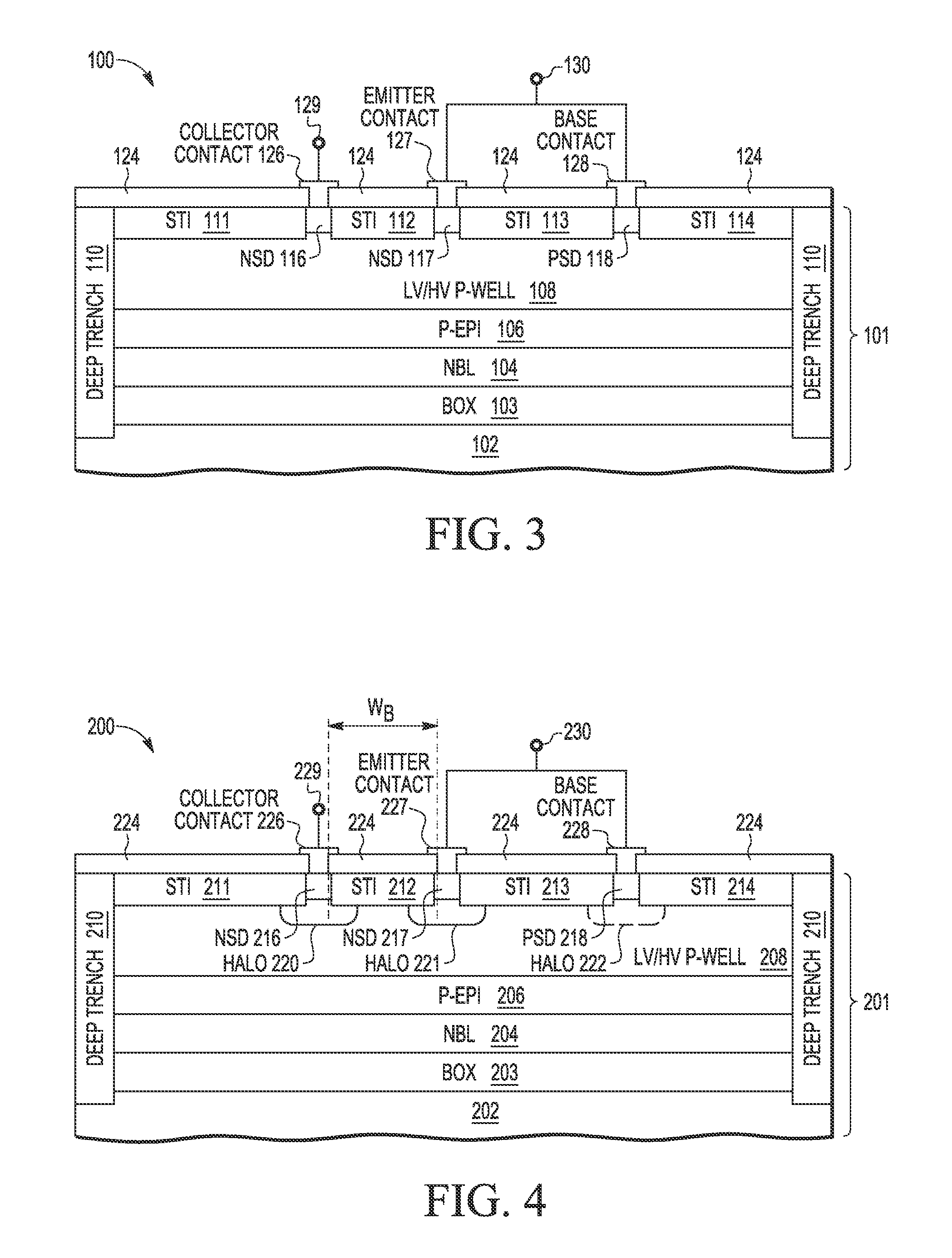
[0016]An NPN-based ESD protection circuit and associated fabrication process are provided for protecting low voltage pins against voltage or current fluctuations. The NPN-based ESD protection circuit uses one or more stacked low voltage NPN bipolar junction transistors, each formed in a p-type material with an N+ collector region and P+ base region formed on opposite sides of an N+ emitter region, and with separate halo extension regions formed around at least the collector and emitter regions to improve the second trigger or breakdown current (It2). This reduced the footprint of the low voltage ESD protection circuits and lowers the susceptibility to rectification without reducing robustness and functionality.

[0017]In selected embodiments, halo extension regions are formed around only the collector and emitter regions with a combination of a shallow n-type LDD extension implant and a heavier and deeper p-type halo implant to surround and enclose the collector and emitter regions, w...


PUM


Abstract

An area-efficient, low voltage ESD protection device (200) is provided for protecting low voltage pins (229, 230) against ESD events by using one or more stacked low voltage NPN bipolar junction transistors, each formed in a p-type material with an N+ collector region (216) and P+ base region (218) formed on opposite sides of an N+ emitter region (217) with separate halo extension regions (220-222) formed around at least the collector and emitter regions to improve the second trigger or breakdown current (It2) and set the snapback voltage (Vsb) and triggering voltage (Vt1) at the desired level.

Description

BACKGROUND OF THE INVENTION[0001]1. Field of the Invention[0002]The present invention is directed in general to integrated circuit devices and methods for manufacturing same. In one aspect, the present invention relates to the manufacture and use of semiconductor devices used for electrostatic discharge (ESD) protection in integrated and other circuits.[0003]2. Description of the Related Art[0004]To protect against electrostatic discharge (ESD) events in integrated circuit devices, ESD protection or clamp devices are typically provided as voltage limiting devices across the inputs and / or other terminals of such integrated circuit devices. ESD protection devices are intended to remain quiescent during normal operation of the associated integrated circuit devices when used with normal operating voltage VO, but turn on when excessive voltage arises, thereby preventing damage to any protected elements in the integrated circuit devices.[0005]Some ESD clamp circuits use bipolar transistor...

Claims


Application Information

Patent Timeline
Patent Type & Authority Applications(United States)
IPC IPC(8): H01L27/02H01L29/735H01L21/266H01L29/08H01L29/10H01L21/762H01L29/66H01L29/06
CPCH01L21/76283H01L27/0259H01L29/6625H01L29/735H01L29/0649H01L29/0808H01L29/0821H01L29/1008
Inventor GILL, CHAI EANHONG, CHANGSOO
Owner NXP USA INC
Learn More