Lens array, method for manufacturing lens array, electro-optical device, and electronic apparatus
a technology of electrooptical devices and lens arrays, applied in the field of lens arrays, can solve the problems of difficult to sufficiently increase the light utilization efficiency and poor light utilization efficiency, and achieve the effect of bright display and high light utilization efficiency
- Summary
- Abstract
- Description
- Claims
- Application Information
AI Technical Summary
Benefits of technology
Problems solved by technology
Method used
Image
Examples
embodiment 1
Electro-Optical Device
[0047]Here, description will be given with an active matrix type liquid crystal device which is provided with a thin film transistor (TFT) as a switching element of a pixel as an example of an electro-optical device. The liquid crystal device is able to be favorably used, for example, as an optical modulator (a liquid crystal light bulb) of a projection type display apparatus (a projector) which will be described below.
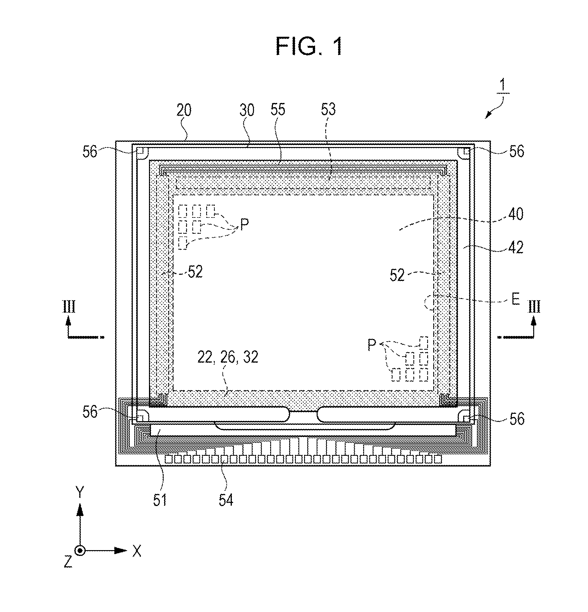
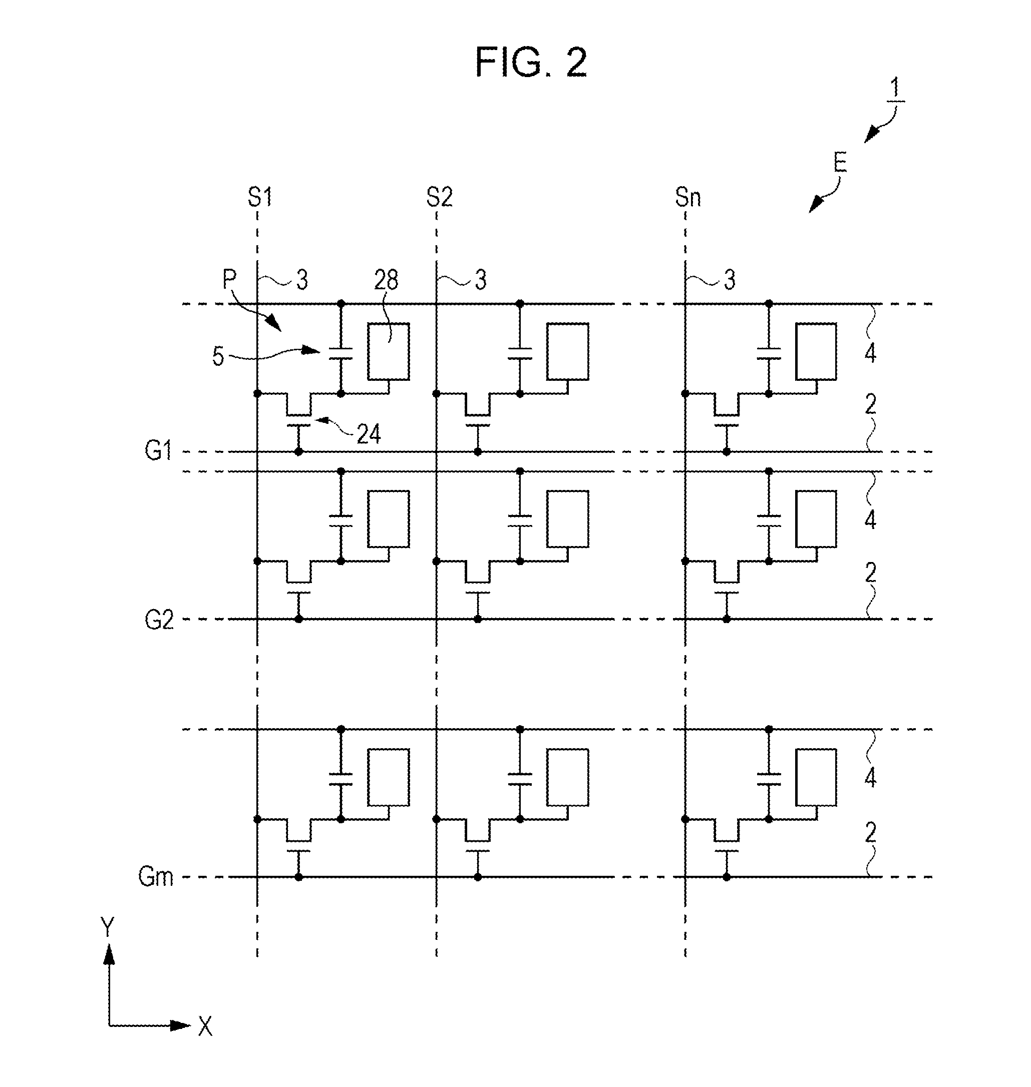
[0048]FIG. 1 is a schematic planar diagram which shows a configuration of a liquid crystal device according to Embodiment 1. FIG. 2 is an equivalent circuit diagram which shows an electrical configuration of the liquid crystal device according to Embodiment 1. FIG. 3 is a schematic cross-sectional diagram which shows a configuration of the liquid crystal device according to Embodiment 1, in detail, a partial schematic cross-sectional diagram taken along line III-III in FIG. 1. Firstly, description will be given of a liquid crystal device 1 accord...
embodiment 2
Form 1 where Unit Cell Group is Different
[0115]FIG. 10 is a diagram which illustrates an example of a microlens array according to Embodiment 2. Next, description will be given of the microlens array 10 according to Embodiment 2 with reference to FIG. 10. Here, the same reference numbers are used for the same configuration sites as Embodiment 1 and overlapping description will be omitted.
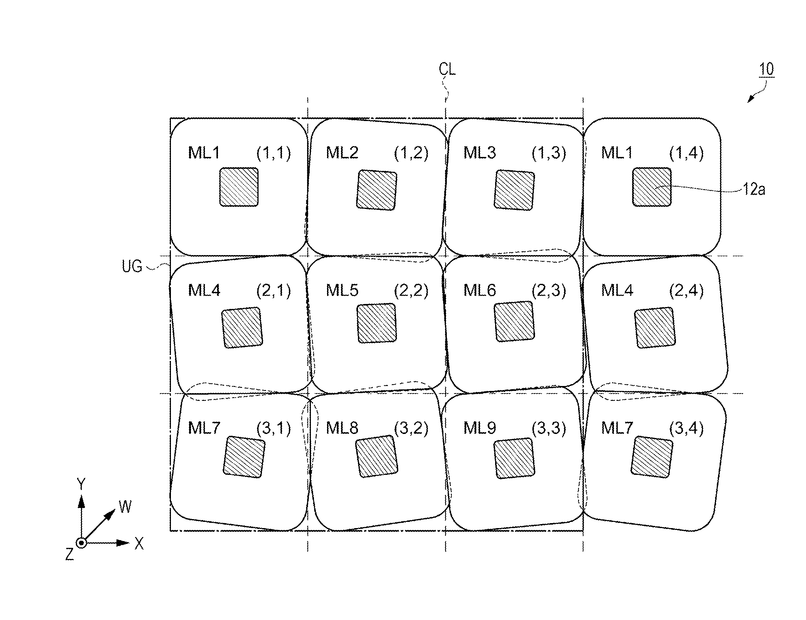
[0116]In the microlens array 10 of the present embodiment shown in FIG. 10, the unit cell groups UG which configure the microlens array 10 are different. Other than this, the microlens array 10 of the present embodiment is the same as Embodiment 1. The unit cell group UG in the microlens array 10 of Embodiment 1 shown in FIG. 6 is configured by 9 different microlenses ML and the unit cell group UG is repeatedly arranged. The configuration of the unit cell group UG is not limited thereto and various forms are possible. For example, as shown in FIG. 10, the unit cell group UG includes the square of n ...
embodiment 3
Form 2 where Unit Cell Group is Different
[0117]FIG. 11 is a diagram which illustrates an example of a microlens array according to Embodiment 3. Next, description will be given of the microlens array 10 according to Embodiment 3 with reference to FIG. 11. Here, the same reference numbers are used for the same configuration sites as Embodiment 1 and overlapping description will be omitted.
[0118]In the microlens array 10 of the present embodiment shown in FIG. 11, the arrangement of the unit cell groups UG which configure the microlens array 10 is different. Other than this, the microlens array 10 of the present embodiment is the same as Embodiment 1. In the microlens array 10 of Embodiment 1 shown in FIG. 6, the unit cell group UG is repeatedly arranged in the X direction and the Y direction. The arrangement of the unit cell group UG is not limited thereto and various forms are possible. For example, as shown in FIG. 11, the unit cell group UG may be arranged by being shifted in each...
PUM
 Abstract
Description
Claims
Application Information
 - R&D
- Intellectual Property
- Life Sciences
- Materials
- Tech Scout
- Unparalleled Data Quality
- Higher Quality Content
- 60% Fewer Hallucinations
Browse by: Latest US Patents, China's latest patents, Technical Efficacy Thesaurus, Application Domain, Technology Topic, Popular Technical Reports.
© 2025 PatSnap. All rights reserved.Legal|Privacy policy|Modern Slavery Act Transparency Statement|Sitemap|About US| Contact US: help@patsnap.com


