
Method of fabricating semiconductor device

Active Publication Date: 2015-06-11
UNITED MICROELECTRONICS CORP
View PDF2 Cites 12 Cited by
  • Summary
  • Abstract
  • Description
  • Claims
  • Application Information

AI Technical Summary

Benefits of technology

The present invention provides a method for making a semiconductor device by using a sacrificial gate process. This method allows for the formation of a gate material layer with a predetermined thickness and eliminates unwanted remaining sacrificial gates. By removing the oxide layer and replacing it with a metal gate, the formed semiconductor device has improved performance and does not include unnecessary materials. This is achieved by using multiple material layer formation processes with a common tool to reduce elapsed time and avoid unwanted oxidation.

Problems solved by technology

With the trend towards scaling down semiconductor devices, however, conventional poly-silicon gates have inferior performances due to boron penetration and an unavoidable depletion effect, which increases the equivalent thickness of the gate dielectric layer, reduces the gate capacitance, and lowers a driving force of the devices.
However, the process deviation, such as too long processing time or improper concentration of the slurry, of the CMP process causes the formed poly-silicon material layer to fail to meet predetermined criteria; for example, the formed poly-silicon material layer has a thickness less than a target thickness, which may further cause some wafers to be scraped to increase the manufacturing cost.

Method used


Image

  • Method of fabricating semiconductor device
  • Method of fabricating semiconductor device
  • Method of fabricating semiconductor device

Examples


Embodiment Construction

[0015]To provide a better understanding of the present invention, preferred exemplary embodiments will be described in detail. The preferred exemplary embodiments of the present invention are illustrated in the accompanying drawings with numbered elements.

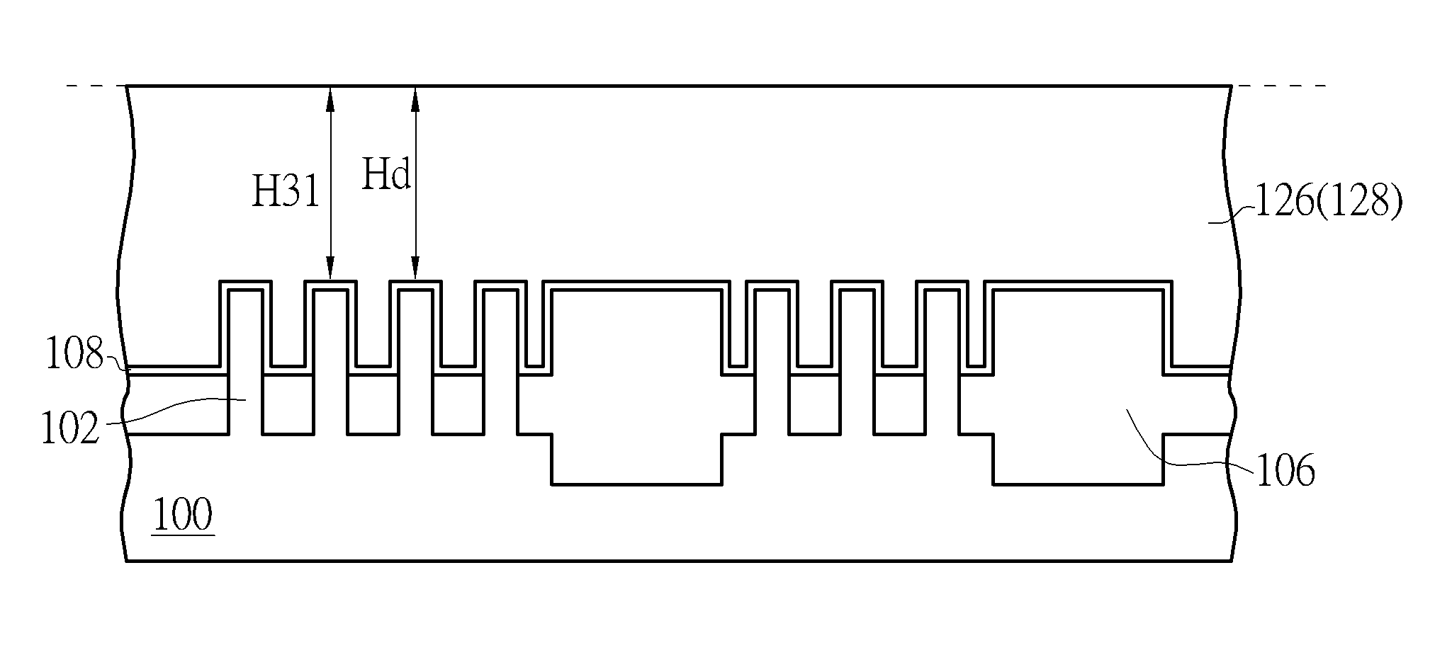
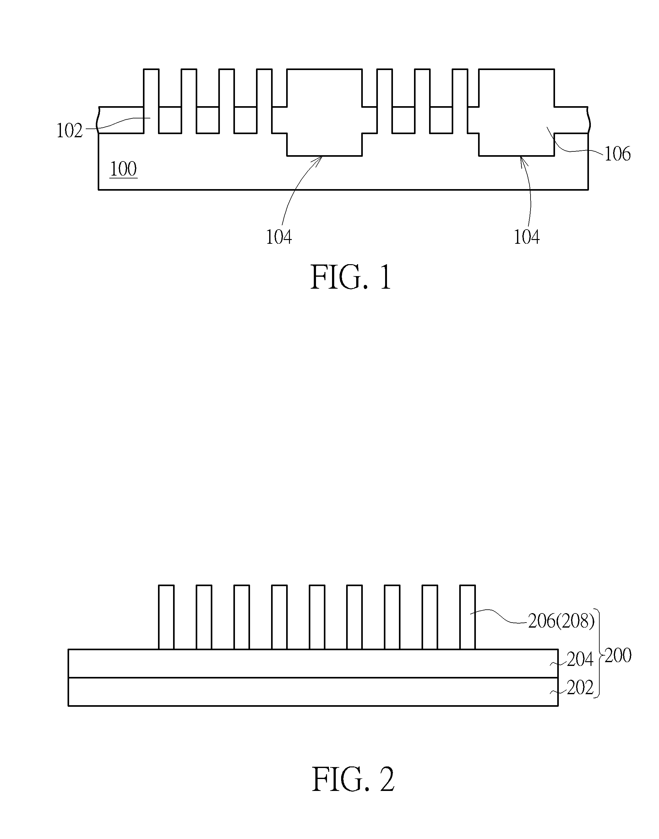
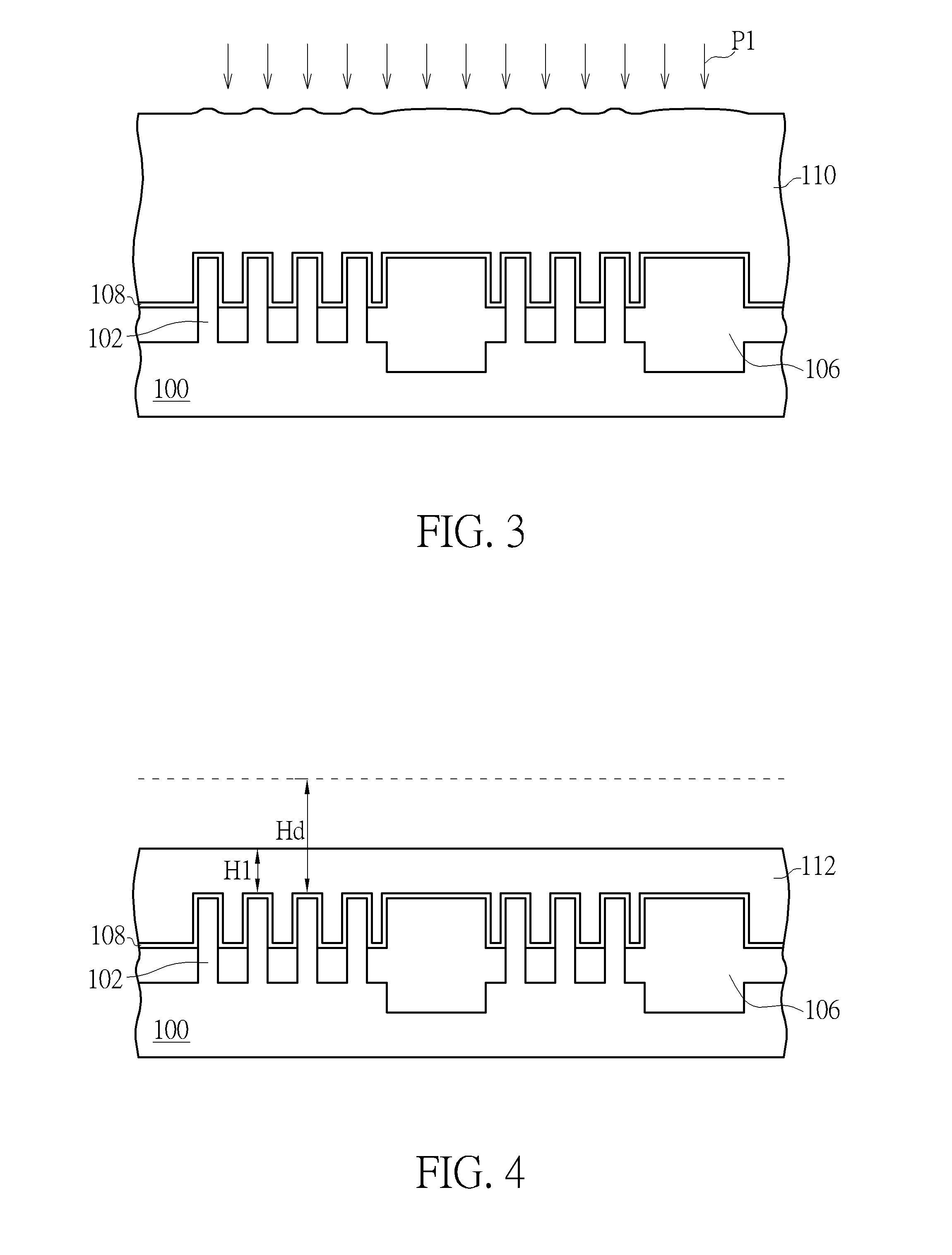
[0016]Please refer to FIG. 1 through FIG. 7, which illustrate a method of forming a semiconductor device according to a first exemplary embodiment of the present invention. As shown in FIG. 1, a substrate 100 is provided, wherein the substrate 100 is a bulk substrate such as a silicon substrate, an epitaxial silicon substrate, a silicon germanium substrate, a silicon carbide substrate or a substrate made of semiconductor material, but is not limited thereto. A mask layer (not shown) is formed on the substrate, wherein the mask layer includes a pad oxide layer (not shown) and a nitride layer (not shown) located on the pad oxide layer. A photolithography process is first performed to pattern the mask layer for forming a patterned pad...


PUM


Abstract

A method of fabricating a semiconductor device includes the following steps. A substrate including at least a fin structure is provided, and a material layer is formed to cover the fin structure. Then, a first planarization process is performed on the material layer to form a first material layer, and an oxide layer is formed on the first material layer. Subsequently, the oxide layer is totally removed to expose the first material layer, and a second material layer is formed in-situ on the first material layer after totally removing the oxide layer.

Description

BACKGROUND OF THE INVENTION[0001]1. Field of the Invention[0002]The present invention relates to a method of fabricating a semiconductor device, and more particularly, to a method of fabricating a semiconductor device which includes a step of removing an oxide layer on a planarized material layer and a step of re-depositing another material layer using the same process tool.[0003]2. Description of the Prior Art[0004]Poly-silicon has been conventionally used as a gate electrode in semiconductor devices, such as metal-oxide-semiconductors (MOS). With the trend towards scaling down semiconductor devices, however, conventional poly-silicon gates have inferior performances due to boron penetration and an unavoidable depletion effect, which increases the equivalent thickness of the gate dielectric layer, reduces the gate capacitance, and lowers a driving force of the devices. Therefore, work function metals are used to replace the conventional poly-silicon gate (which acts as a sacrificia...

Claims


Application Information

Patent Timeline
IPC IPC(8): H01L29/66H01L21/321H01L21/02H01L21/3205
CPCH01L29/66545H01L21/32055H01L21/02318H01L21/02112H01L21/3212H01L21/02074H01L29/66795
Inventor LI, YU-TINGHUANG, PO-CHENGSIE, WU-SIANWANG, CHUN-HSIUNGLIU, YI-LIANGHSU, CHIA-LINHUANG, RAI-MIN
Owner UNITED MICROELECTRONICS CORP
Learn More