Liquid crystal element and liquid crystal display apparatus
a liquid crystal element and liquid crystal display technology, applied in static indicating devices, instruments, non-linear optics, etc., can solve the problems of inverse twist orientation state, increase threshold voltage, switch element and electrode structure, etc., to improve contrast ratio and low power consumption
- Summary
- Abstract
- Description
- Claims
- Application Information
AI Technical Summary
Benefits of technology
Problems solved by technology
Method used
Image
Examples
embodiment 1
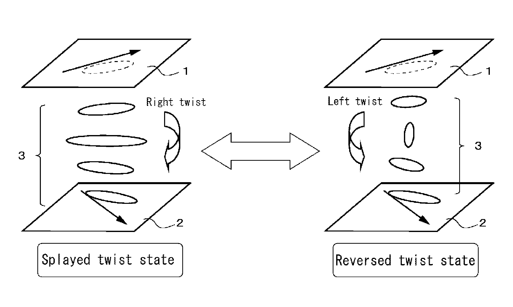
[0056]FIG. 9 is a cross-sectional view showing a configuration example of the R-TN mode liquid crystal element of embodiment 1. Further, FIG. 10 is a plan view of the R-TN mode liquid crystal element shown in FIG. 9. It should be noted that FIG. 9 shows a cross-section along a line a-a shown in FIG. 10. The R-TN mode liquid crystal element of this embodiment shown in each figure is configured to comprise a first substrate (lower substrate) 11, a second substrate (upper substrate) 12, a first electrode 13, a common line 14, a scan line 15, an insulation film 16, a semiconductor film 17, a source electrode 18, a drain electrode 19, a second electrode 20, a first alignment film 21, a second alignment film 22, a common electrode 23, a liquid crystal layer 24, a signal line 25, an insulation film 26, a first polarizing plate (lower polarizing plate) 31, and a second polarizing plate (upper polarizing plate) 32.
[0057]The first substrate 11 and the second substrate 12 are disposed facing e...
embodiment 2
[0090]FIG. 13 is a cross-sectional view showing a configuration example of the R-TN mode liquid crystal element of embodiment 2. Further, FIG. 14 is a plan view of the R-TN mode liquid crystal element shown in FIG. 13. It should be noted that FIG. 13 shows a cross-section along a line b-b shown in FIG. 14. The R-TN mode liquid crystal element of this embodiment shown in each figure is configured to comprise the first substrate (lower substrate) 11, the second substrate (upper substrate) 12, the first electrode 13, a common line 14a, the scan line 15, the insulation film 16, the semiconductor film 17, the source electrode 18, the drain electrode 19a, the second electrode (pixel electrode) 20, the first alignment film 21, the second alignment film 22, the common electrode 23, the liquid crystal layer 24, the signal line 25, the first polarizing plate (lower polarizing plate) 31, and the second polarizing plate (upper polarizing plate) 32. It should be noted that the components common ...
embodiment 3
[0108]FIG. 17A is a cross-sectional view schematically showing a configuration example of the R-TN mode liquid crystal element of embodiment 3. The R-TN mode liquid crystal element of embodiment 3 shown in FIG. 17A is a reflective liquid crystal element that displays images utilizing external light, and comprises a liquid crystal panel 50, a reflective plate 51 disposed on the lower surface side of this liquid crystal panel 50, a scattering plate 52 disposed on the upper surface side of the liquid crystal panel 50, a λ / 4 wavelength plate 53 disposed overlapping with this scattering plate 52, and a polarizing plate 54 disposed overlapping with this λ / 4 wavelength plate 53. As the reflective plate 51, a silver film can be used, for example. Further, as the scattering plate 52, a plurality of overlapping plates with a haze value of 43-45% can be used, for example. Further, as the λ / 4 wavelength plate 53, a plate with a phase difference of approximately 137 nm can be used, for example. ...
PUM
| Property | Measurement | Unit |
|---|---|---|
| angle | aaaaa | aaaaa |
| angle | aaaaa | aaaaa |
| pretilt angle | aaaaa | aaaaa |
Abstract
Description
Claims
Application Information
 - R&D
- Intellectual Property
- Life Sciences
- Materials
- Tech Scout
- Unparalleled Data Quality
- Higher Quality Content
- 60% Fewer Hallucinations
Browse by: Latest US Patents, China's latest patents, Technical Efficacy Thesaurus, Application Domain, Technology Topic, Popular Technical Reports.
© 2025 PatSnap. All rights reserved.Legal|Privacy policy|Modern Slavery Act Transparency Statement|Sitemap|About US| Contact US: help@patsnap.com


