
Organic light-emitting display apparatus and method of manufacturing the same

a technology of light-emitting display and organic materials, which is applied in the direction of electrical devices, thermoelectric device junction materials, and semiconductor devices, can solve the problems of manufacturing procedure safety degradation, and achieve the effect of excellent adsorption performance and manufacturing procedure safety

Inactive Publication Date: 2014-12-11
SAMSUNG DISPLAY CO LTD
View PDF3 Cites 34 Cited by
  • Summary
  • Abstract
  • Description
  • Claims
  • Application Information

AI Technical Summary

Benefits of technology

The invention provides an organic light-emitting display with a multi-layered pixel electrode that has excellent adsorbing performance and manufacturing safety. The pixel electrode includes a fourth layer with a high work function. This improves the display's performance and ensures the manufacturing process is secure.

Problems solved by technology

However, the aforementioned ITO / Ag / ITO structure may cause Ag conglomeration, and the safety of the manufacturing procedure may deteriorate due to the different etch rates of ITO and Ag.

Method used


Image

  • Organic light-emitting display apparatus and method of manufacturing the same
  • Organic light-emitting display apparatus and method of manufacturing the same
  • Organic light-emitting display apparatus and method of manufacturing the same

Examples


Embodiment Construction

[0033]Hereinafter, exemplary embodiments of the present invention will be described in detail by explaining exemplary embodiments of the invention with reference to the attached drawings. Exemplary embodiments of the invention may, however, be embodied in many different forms and should not be construed as being limited to exemplary embodiments set forth herein. Like reference numerals in the drawings denote like or similar elements throughout the specification.

[0034]It will be understood that when a layer, a film, a region, a plate, or the like is referred to as being “on” another layer, film, region, or plate, the layer, film, region, or plate can be directly on another layer, film, region, or plate or an intervening layer, film, region, or plate may also be present.

[0035]In the drawings, the thicknesses of layers and regions may be exaggerated for clarity.

[0036]As used herein, the term “and / or” includes any and all combinations of one or more of the associated listed items. In ad...


PUM


Abstract

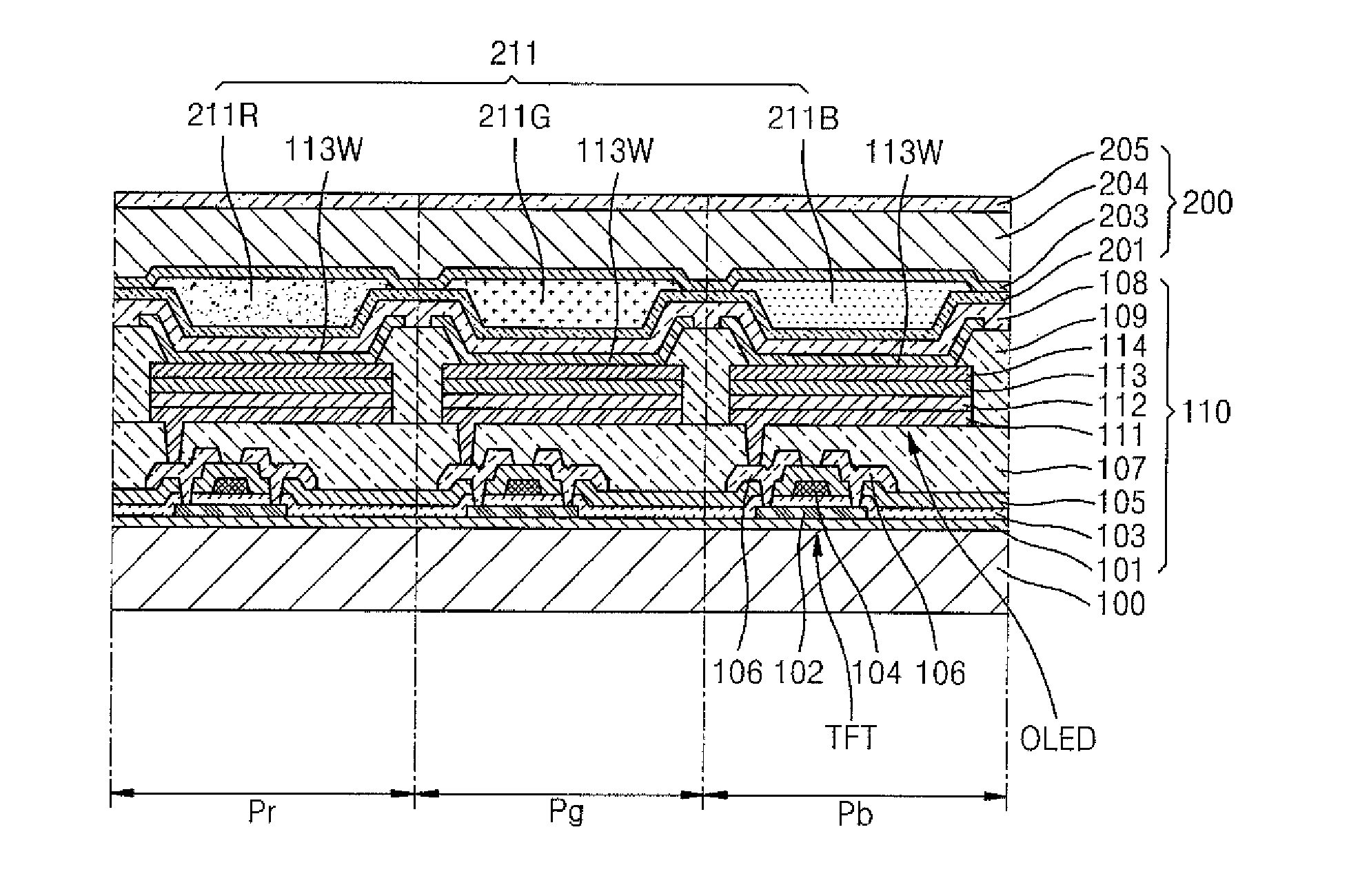
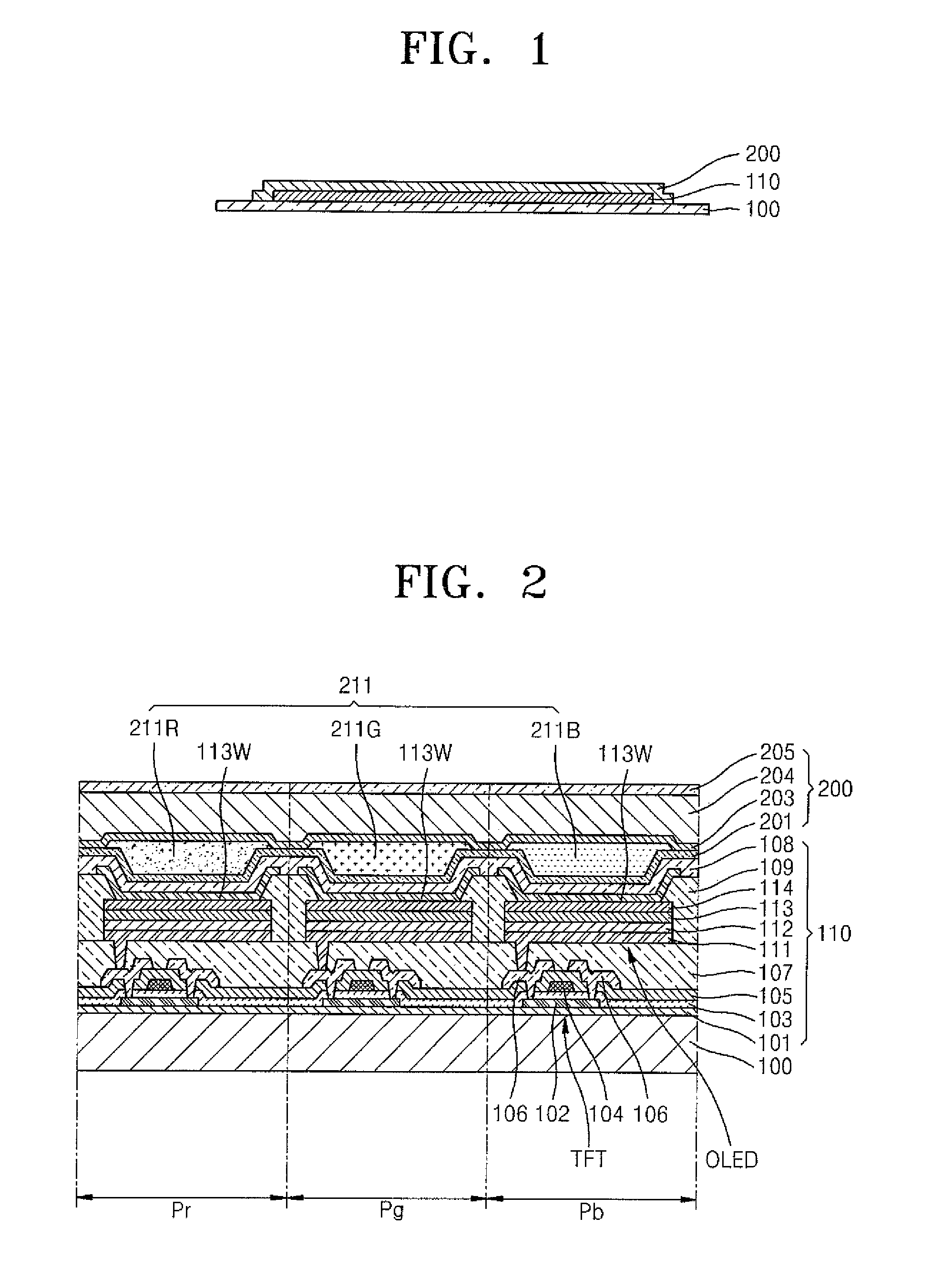
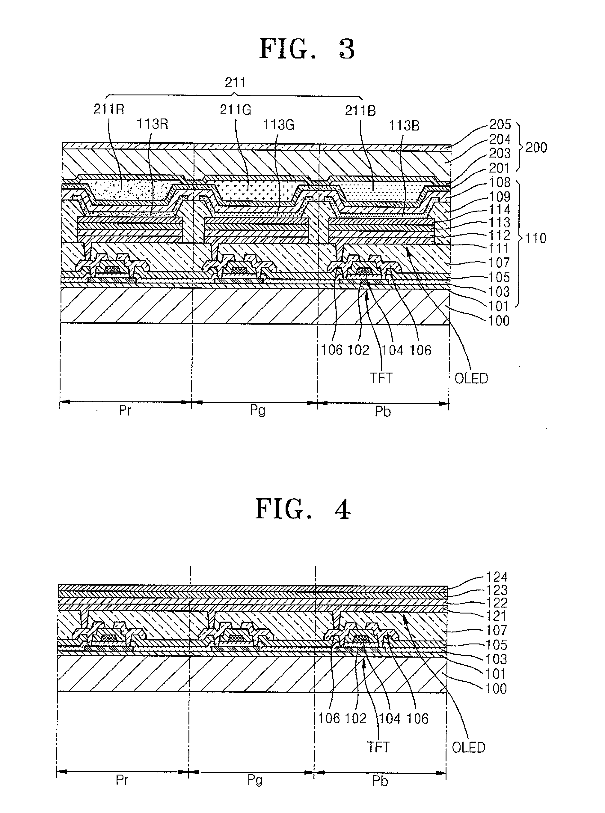
An organic light-emitting display apparatus includes a substrate, a thin film transistor (TFT) disposed on the substrate and including an active layer, a gate electrode, a source electrode, and a drain electrode The organic light-emitting display apparatus further includes a pixel electrode including a first pixel electrode layer, a second pixel electrode layer disposed on the first pixel electrode layer and a third pixel electrode layer disposed on the second pixel electrode layer. The second pixel electrode layer is a metal layer and the third pixel electrode layer is a reflective layer. The organic light-emitting display apparatus further includes an emission layer (EML) disposed on the pixel electrode, and an opposite layer disposed on the EML.

Description

CROSS-REFERENCE TO RELATED PATENT APPLICATION [0001]This application claims priority to Korean Patent Application No. 10-2013-0065464, filed on Jun. 7, 2013, the disclosure of which is hereby incorporated by reference herein in its entirety.TECHNICAL FIELD [0002]The present disclosure relates to an organic light-emitting display apparatus and a method of manufacturing the same, and more particularly, to an organic light-emitting display apparatus having a multi-layered pixel electrode, and a method of manufacturing the organic light-emitting display apparatus.DISCUSSION OF THE RELATED ART [0003]Recently, conventional display devices have started to be replaced with portable, thin flat panel display devices. Among the flat panel display devices, organic or inorganic display devices are self-emissive display devices which may have, for example, a wide viewing angle, an excellent contrast ratio, and a high response time. Thus, the above-mentioned flat panel display devices are regarded...

Claims


Application Information

Patent Timeline
Patent Type & Authority Applications(United States)
IPC IPC(8): H01L27/32H01L51/00H01L51/56
CPCH01L27/3248H01L51/56H01L51/0021H10K59/38H10K59/125H10K59/80518H10K59/8731H10K59/123H10K59/122H10K59/1213H10K50/818H10K59/12
Inventor CHOI, JIN-BAEKCHOUNG, JI-YOUNGLEE, YEON-HWAKIM, WON-JONGBANG, HYUN-SUNGLEE, JOON-GU
Owner SAMSUNG DISPLAY CO LTD
Learn More