Memory device and method for high speed and reliability
a memory device and high speed technology, applied in the field of memory devices, can solve the problems of unreliable existing flash memory devices, inability to inability of existing memory devices to perform read, program or erase to multiple memories with only one instruction, etc., to achieve high processing performance and high reliability
- Summary
- Abstract
- Description
- Claims
- Application Information
AI Technical Summary
Benefits of technology
Problems solved by technology
Method used
Image

Examples
first embodiment
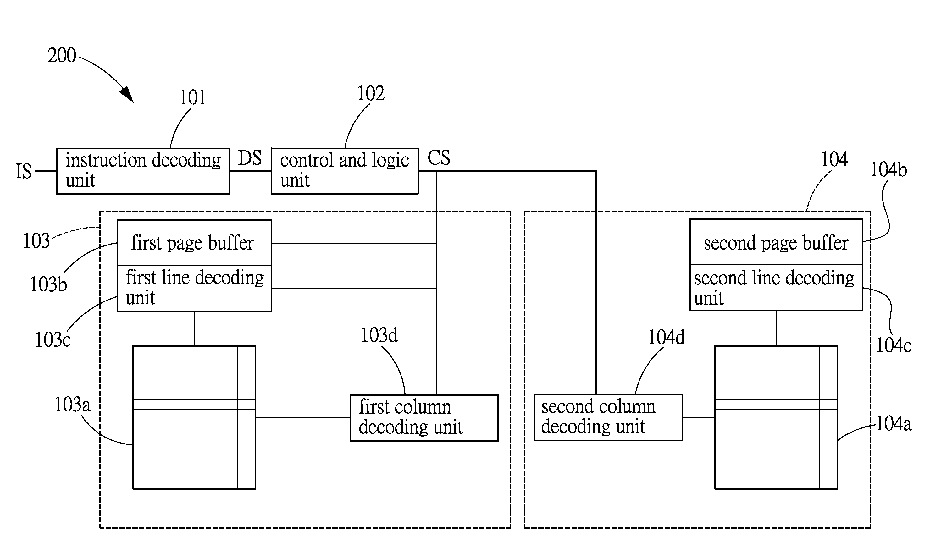
[0030]Referring to FIGS. 2A, a memory device 200 in accordance with the present invention is shown and comprises: an instruction decoding unit 101, a control and logic unit 102, a first memory 103 and a second memory 104.
[0031]It is to be noted that the memory device 200 of the first embodiment of the present invention is a NAND flash memory, and can also be a solid state disk (SSD) or in any other available forms.
[0032]The first memory 103 includes a first memory array 103a and a first page buffer 103b, and the second memory 104 includes a second memory array 104a and a second page buffer 104b. The first page buffer 103b is connected to the control and logic unit 102 and the first memory array 103a, and the second page buffer 104b is connected to the control and logic unit 102 and the second logic array 104a.
[0033]When the instruction decoding unit 101 receives an IS (inputted instruction), it will produce a DS (decoding signal) based on the IS, then the control and logic unit 102...
second embodiment
[0037]Referring then to FIG. 2B, which shows a memory device in accordance with the present invention, wherein the control and logic unit 102 comprises a decision unit 102a connected to the instruction decoding unit 101, and the decision unit 102a is used to decide whether the IS is a PS or a NS.
[0038]It is to be noted that, when the IS is PS, the DS will include an ES1 (enable signal) and an ES2.
[0039]In a preferred embodiment, the decision unit 102a further comprises a first AND gate 21 and a second AND gate 22. The first AND gate 21 has a first end connected to the instruction decoding unit 101 to receive an Address code A and has a second end connected to the ES1. The second AND gate 22 has a first end connected to the instruction decoding unit 101 to receive the address code A and has a second end connected to the ES2.
third embodiment
[0040]Referring then to FIG. 3A, a memory device 200 in accordance with the present invention is reading a Page of data simultaneously from two memory arrays via a PS (preset instruction). The decision unit 102a of this embodiment employs the first AND gate 21 and the second AND gate 22 to decide whether it is a PS.
[0041]In a preferred embodiment, when the IS is a PS, and the PS is decoded by the instruction decoding unit 101, the ES1 and ES2 will become the signal of a logic 1. Therefore, the first and second AND gates 21, 22 will select and enable a page of the memory arrays 103a, 104a via the address code A of the DS. In other words, the memory device 200 selects the page to be read via the address code 11b, then the address code A simultaneously enables the first memory array 103a, the first page buffer 103b, the second memory array 104a and the second page buffer 104b, namely, enabling the first and second memories 103, 104 to perform read operation simultaneously, and then the...
PUM
 Abstract
Description
Claims
Application Information
 - R&D
- Intellectual Property
- Life Sciences
- Materials
- Tech Scout
- Unparalleled Data Quality
- Higher Quality Content
- 60% Fewer Hallucinations
Browse by: Latest US Patents, China's latest patents, Technical Efficacy Thesaurus, Application Domain, Technology Topic, Popular Technical Reports.
© 2025 PatSnap. All rights reserved.Legal|Privacy policy|Modern Slavery Act Transparency Statement|Sitemap|About US| Contact US: help@patsnap.com