Electro-optic device and electronic device
- Summary
- Abstract
- Description
- Claims
- Application Information
AI Technical Summary
Benefits of technology
Problems solved by technology
Method used
Image
Examples
embodiment
A: Embodiment
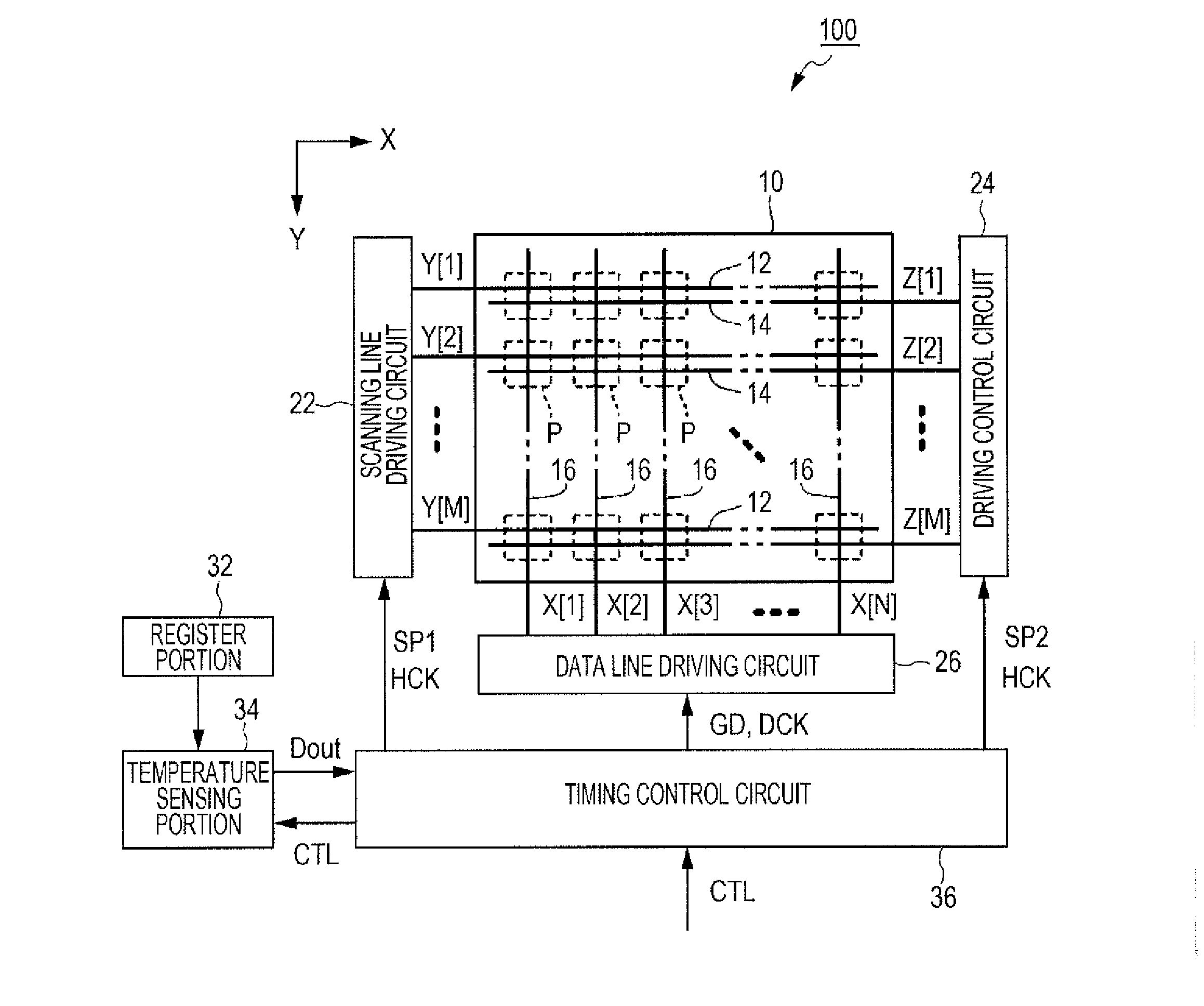
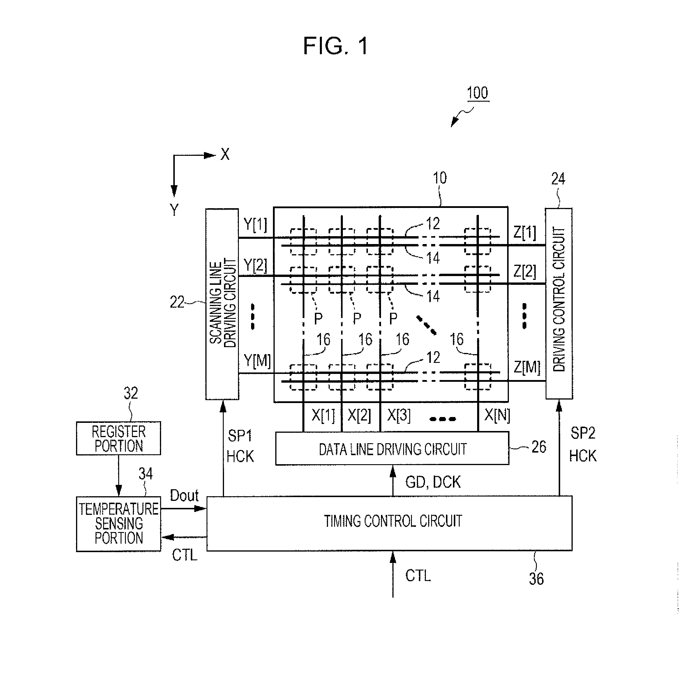
[0030]FIG. 1 is a block diagram illustrating a configuration of an electro-optic device (a display device) according to an embodiment of the invention. As shown in FIG. 1, an electro-optic device 100 includes an element array portion 10 in which a plurality of pixel circuits P is arranged, a scanning line driving circuit 22, a driving control circuit 24, a data line driving circuit 26, a register portion 32 which stores therein various pieces of setting data, a temperature sensing portion 34 which detects temperatures and specifies a period during which electro-optic elements emit light. These constitutive elements are preferred to be formed on a single-crystalline silicon substrate. Further, the electro-optic device 100 is controlled by a lighting control signal CTL supplied from an external device with respect to whether image display operation is to be performed or not to be performed. Further, during a first period when image display operation is not to be performed...
modification example
B: Modification Example
[0076]various modifications can be made on the aforementioned embodiment. Specific embodiments of such modifications will be exemplified below. In addition, any ones of embodiments described below may be appropriately combined.
modification example 1
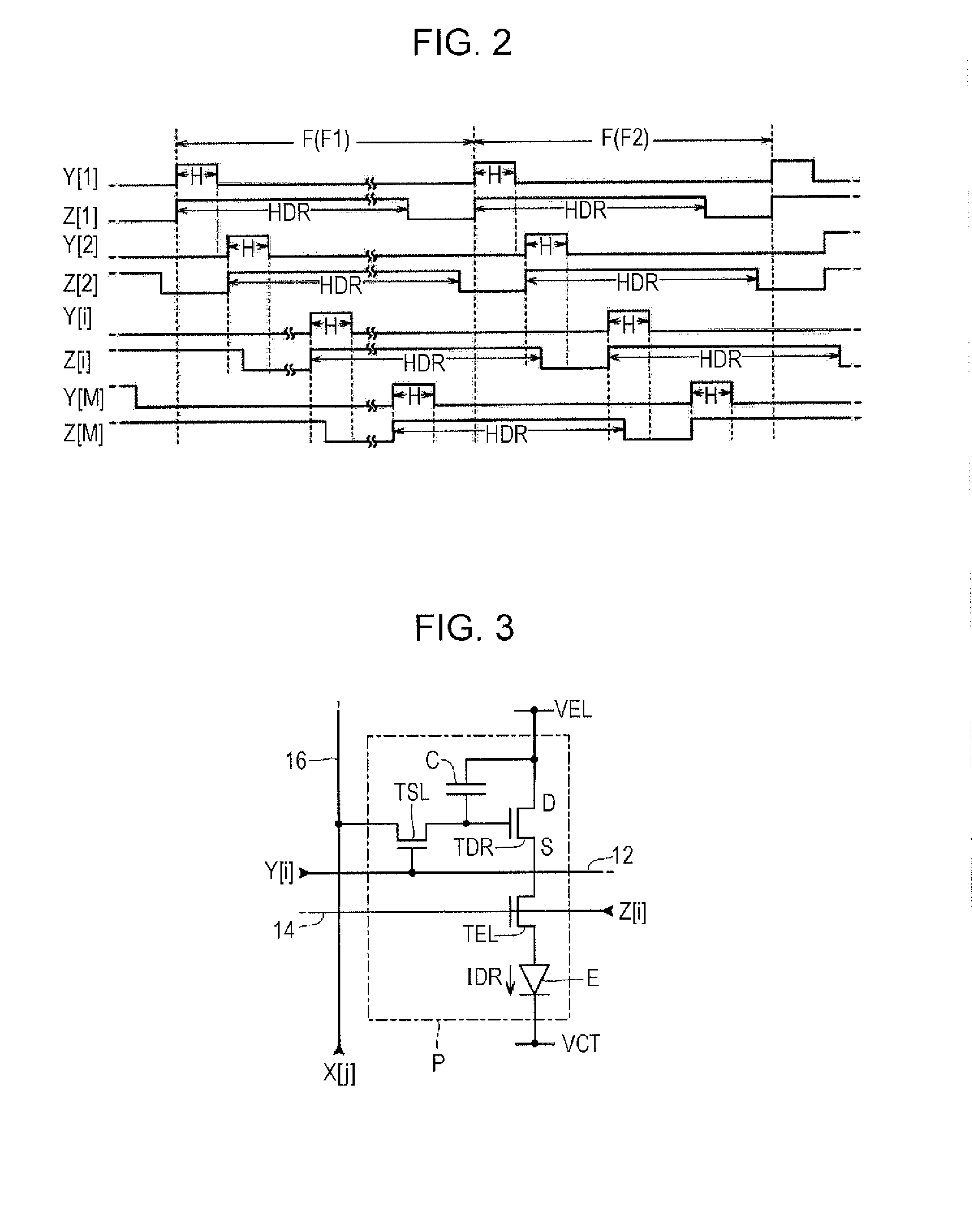
[0077]Although, in the aforementioned embodiment, there is exemplified the configuration in which the driving control transistor TEL is caused in the conductive state simultaneously with the start of the writing period H, the timing point of causing the driving control transistor TEL to be in the conductive state (i.e., the timing point of setting the driving control signal Z [i] to H-level) can be appropriately changed to a different timing point. For example, the driving control transistor TEL may be caused in the conductive state from a timing point before or after the start of the writing period H. Further, the driving control transistor TEL may be caused in the conductive state from a timing point of the completion of the writing period H. Moreover, the light emitting period HDR may be started at a timing point after elapse of a given period of time from the completion of the writing period H, and may be terminated at a timing point immediately before a next writing period H.
PUM
 Abstract
Description
Claims
Application Information
 - R&D
- Intellectual Property
- Life Sciences
- Materials
- Tech Scout
- Unparalleled Data Quality
- Higher Quality Content
- 60% Fewer Hallucinations
Browse by: Latest US Patents, China's latest patents, Technical Efficacy Thesaurus, Application Domain, Technology Topic, Popular Technical Reports.
© 2025 PatSnap. All rights reserved.Legal|Privacy policy|Modern Slavery Act Transparency Statement|Sitemap|About US| Contact US: help@patsnap.com


