Liquid crystal display device and liquid crystal panel drive method
一种液晶显示、液晶面板的技术,应用在静态指示器、仪器等方向,能够解决显示图像质量下降、闪烁电势未得到解决等问题,达到抑制闪烁的效果
- Summary
- Abstract
- Description
- Claims
- Application Information
AI Technical Summary
Problems solved by technology
Method used
Image
Examples
no. 1 example
[0047] 4 is a block diagram showing a schematic structure of a liquid crystal panel driving module of a liquid crystal display device according to a first exemplary embodiment of the present invention.
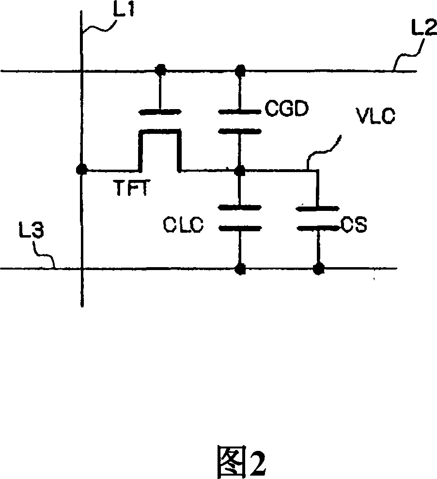
[0048] Referring to FIG. 4, the liquid crystal panel driving module can drive the liquid crystal panel 16, and can include the following as its main components: V-T / gamma correction circuit 10; switching circuit 11; look-up tables (LUT) 12a and 12b; liquid crystal driving circuit 13; a control signal generating module 14; and a common voltage generating circuit 15. The liquid crystal panel 16 may include an off-the-shelf liquid crystal panel, and may be, for example, the same as the liquid crystal panel shown in FIG. 2 . Switching circuit 11 and look-up tables (LUTs) 12a and 12b may include components for adjusting the brightness of a displayed image (eg, may include an adjustment module).
[0049] The V-T / gamma correction circuit 10 may have the same structure as the V-T / gam...
no. 2 example
[0076] 6 is a block diagram showing a schematic structure of a liquid crystal panel driving module of a liquid crystal display device according to a second exemplary embodiment of the present invention. The difference between the liquid crystal panel driving module shown in FIG. 6 and the structure shown in FIG. 4 is that LUT20 and offset table 21 are provided instead of switching circuit 11 and LUT12a and 12b. The V-T / gamma correction circuit 10, the control signal generation block 14, and the common voltage generation circuit 15 are the same as those shown in FIG. 4 .
[0077] Characteristic data for adjusting brightness of a display image related to image data of positive polarity or negative polarity may be stored in the LUT 20 . In the offset table 21, characteristic data for returning (shifting) the image data in which the luminance has been adjusted by the characteristic data of the LUT 20 to the image data of the luminance before adjustment can be stored.
[0078] Ima...
no. 3 example
[0083] 7 is a block diagram showing a schematic structure of a liquid crystal panel driving module of a liquid crystal display device according to a third exemplary embodiment of the present invention. The difference between the liquid crystal panel driving module shown in FIG. 7 and the structure shown in FIG. 4 is that a V-T correction circuit 30 and gamma correction circuits 31a and 31b are provided to replace the V-T / gamma correction circuit 10 and LUTs 12a and 12b. The control signal generating block 14 and the common voltage generating circuit 15 are the same as those shown in FIG. 4 .
[0084] The V-T correction circuit 30 is basically the same as the V-T correction circuit making up the V-T / gamma correction circuit 10, and is composed of LUTs. FIG. 8A shows an example of characteristic data of an LUT used for V-T correction in the V-T correction circuit 30 . The vertical axis is output (V), and the horizontal axis is input (V). These characteristic data include data ...
PUM
 Abstract
Description
Claims
Application Information
 - R&D
- Intellectual Property
- Life Sciences
- Materials
- Tech Scout
- Unparalleled Data Quality
- Higher Quality Content
- 60% Fewer Hallucinations
Browse by: Latest US Patents, China's latest patents, Technical Efficacy Thesaurus, Application Domain, Technology Topic, Popular Technical Reports.
© 2025 PatSnap. All rights reserved.Legal|Privacy policy|Modern Slavery Act Transparency Statement|Sitemap|About US| Contact US: help@patsnap.com


