Optical element, optical system and optical apparatus having antireflection coating
a technology of optical elements and coatings, applied in the field of optical elements, optical systems and optical apparatuses, can solve the problems of remarkably deteriorating anti-reflection performance, and achieve the effect of good wavelength band characteristi
- Summary
- Abstract
- Description
- Claims
- Application Information
AI Technical Summary
Benefits of technology
Problems solved by technology
Method used
Image
Examples
first embodiment
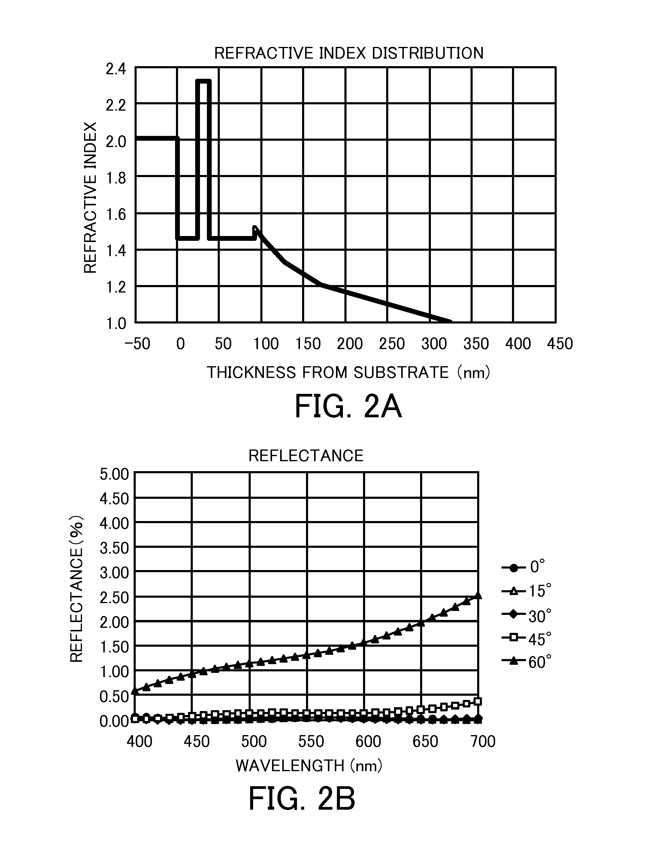
[0042]FIG. 2A is a graph illustrating a refractive index distribution of an antireflection coating 100 according to a first embodiment. The abscissa axis is a thickness (nm) from a surface of a substrate 10 and the ordinate axis is a refractive index. The abscissa and ordinate axes in other embodiments are similarly defined. A region where the thickness from the surface of the substrate is 0 or less corresponds to the substrate 10. Table 1 summarizes a configuration of the antireflection coating 100 according to the first embodiment. In Table 1, n denotes a refractive index, d denotes a physical thickness, and nd (n×d) denotes an optical thickness. These notations are applicable to corresponding tables in other embodiments.
TABLE 1nd(nm)ndFineundulation1 −> 1.52221—UndulationportionstructurehomogeneousportionIntermediatethird layer1.465479layersecond layer2.321433first layer1.462435Optical substrate2.01——
[0043]The antireflection coating 100 according to the first embodiment is formed...
second embodiment
[0046]FIG. 3A is a graph illustrating a refractive index distribution of an antireflection coating 100 according to a second embodiment. Table 2 summarizes a configuration of the antireflection coating 100 according to the second embodiment.
TABLE 2nd(nm)ndFineundulation1 −> 1.52288—Undulationportionstructurehomogeneous1.524975portionIntermediatethird layer1.461319layersecond layer2.032755first layer1.461928Optical substrate1.97——
[0047]The antireflection coating 100 according to the second embodiment is formed on the substrate 10 with a refractive index of 1.97. The intermediate layer 20 includes, in order from the substrate, a first layer that has a physical thickness of 19 nm, is made of SiO2 as its primary ingredient, and has a refractive index of 1.46, a second layer that has a physical thickness of 27 nm, is made of Ta2O2 as its primary ingredient, and has a refractive index of 2.03, and a third layer that has a physical thickness of 13 nm, is made of SiO2 as its primary ingredi...
third embodiment
[0054]FIG. 4A is a graph illustrating a refractive index distribution of an antireflection coating 100 according to a third embodiment. Table 3 summarizes a configuration of the antireflection coating 100 according to the third embodiment.
TABLE 3nd(nm)ndFineundulation1 −> 1.52221—Undulationportionstructurehomogeneous1.525685portionIntermediatethird layer1.460 0layersecond layer2.032041first layer1.632541Optical substrate2.01——
[0055]The antireflection coating 100 according to the third embodiment is formed on the substrate 10 with a refractive index of 2.01. The intermediate layer 20 includes, in order from the substrate, a first layer that has a physical thickness of 25 nm, is made of Al2O3 as its primary ingredient, and has a refractive index of 1.65, and a second layer that has a physical thickness of 20 nm, is made of Ta2O5 as its primary ingredient, and has a refractive index of 2.03. The intermediate layer 20 according to the third embodiment does not include a third layer. The...
PUM
| Property | Measurement | Unit |
|---|---|---|
| Thickness | aaaaa | aaaaa |
| Thickness | aaaaa | aaaaa |
| Thickness | aaaaa | aaaaa |
Abstract
Description
Claims
Application Information
 - R&D
- Intellectual Property
- Life Sciences
- Materials
- Tech Scout
- Unparalleled Data Quality
- Higher Quality Content
- 60% Fewer Hallucinations
Browse by: Latest US Patents, China's latest patents, Technical Efficacy Thesaurus, Application Domain, Technology Topic, Popular Technical Reports.
© 2025 PatSnap. All rights reserved.Legal|Privacy policy|Modern Slavery Act Transparency Statement|Sitemap|About US| Contact US: help@patsnap.com


