Thin-film transistor substrate and method of manufacturing the thin-film transistor substrate

a technology of thin film transistors and substrates, which is applied in the direction of semiconductor/solid-state device manufacturing, electrical equipment, semiconductors, etc., can solve the problems of undesirably low aperture ratio of pixels and undesirable contact holes, and achieve the effect of reducing manufacturing costs and manufacturing time, and simplifying the manufacturing of thin film transistor substrates

Active Publication Date: 2014-05-29
SAMSUNG DISPLAY CO LTD
View PDF11 Cites 11 Cited by
  • Summary
  • Abstract
  • Description
  • Claims
  • Application Information

AI Technical Summary

Benefits of technology

[0010]One or more embodiments of the present invention may be related to a thin film transistor substrate that includes the following elements: a base substrate, a data line disposed on the base substrate and configured to transmit a data signal, a source electrode (directly) contacting the data line, a drain electrode spaced from the source electrode, a channel disposed between the source electrode and the drain electrode, a pixel electrode electrically connected to the drain electrode, a gate insulation pattern disposed on the channel, and a gate electrode disposed on the gate insulation pattern. In the thin film transistor substrate, only one contact hole may be required for each pixel. Advantageously, the aperture ratio of each pixel may be sufficiently large to provide satisfactory image quality. In the thin film transistor substrate, the source electrode, the drain electrode, and the pixel electrode may be in a same layer and may be formed in a same process using a same mask. Therefore, manufacturing of the thin film transistor substrate may be simplified. Advantageously, manufacturing cost and manufacturing time for the thin film transistor substrate may be minimized.
[0019]One or more embodiments of the present invention may be related to a method of manufacturing a thin film transistor substrate. The method may include the following steps: forming a data line on a base substrate; forming a data insulation layer on the data line, wherein the data insulation layer exposes a portion of the data line; forming a semiconductor layer on the data insulation layer; patterning the semiconductor layer to form a semiconductor pattern that contacts the data line; forming a gate insulation pattern the semiconductor pattern; forming a gate electrode on the gate insulation pattern, wherein at least one of the gate insulation pattern and the gate electrode covers a first portion of the semiconductor pattern without covering a second portion of the semiconductor pattern; and processing the second portion of the semiconductor pattern to form a source electrode that (directly) contacts the portion of the data line, a drain electrode that is spaced from the source electrode, and a pixel electrode that is electrically connected to the drain electrode. In the method, the source electrode, the drain electrode, and the pixel electrode may be formed in a same process using a same mask. Therefore, manufacturing of the thin film transistor substrate may be simplified. Advantageously, manufacturing cost and manufacturing time for the thin film transistor substrate may be minimized.

Problems solved by technology

The requirement of at least two contact holes may be undesirable, especially for a high-resolution display apparatus that requires small pixels.
For example, the requirement of at least two contact holes may lead to an undesirably low aperture ratio of the pixels.

Method used


Image

  • Thin-film transistor substrate and method of manufacturing the thin-film transistor substrate
  • Thin-film transistor substrate and method of manufacturing the thin-film transistor substrate
  • Thin-film transistor substrate and method of manufacturing the thin-film transistor substrate

Examples


Embodiment Construction

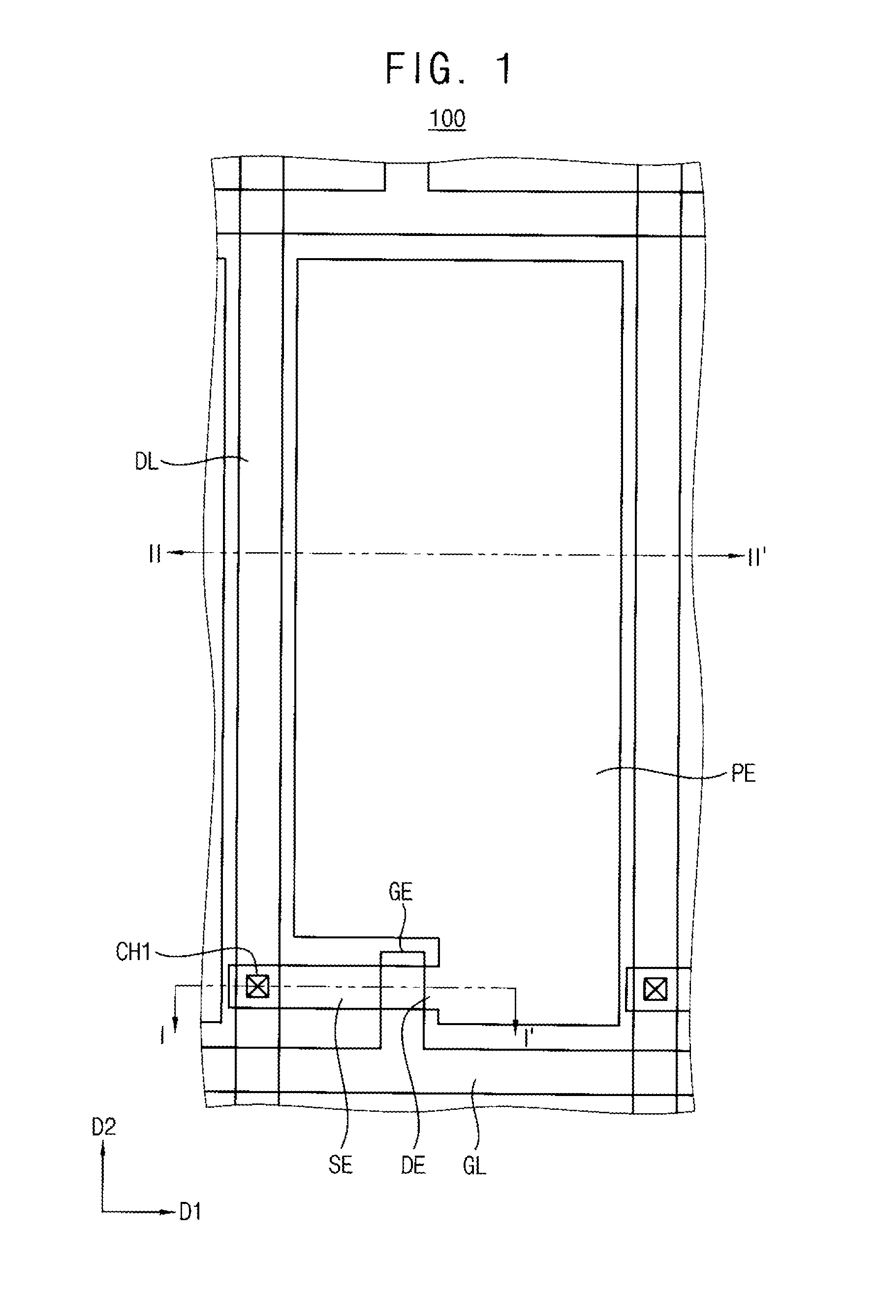
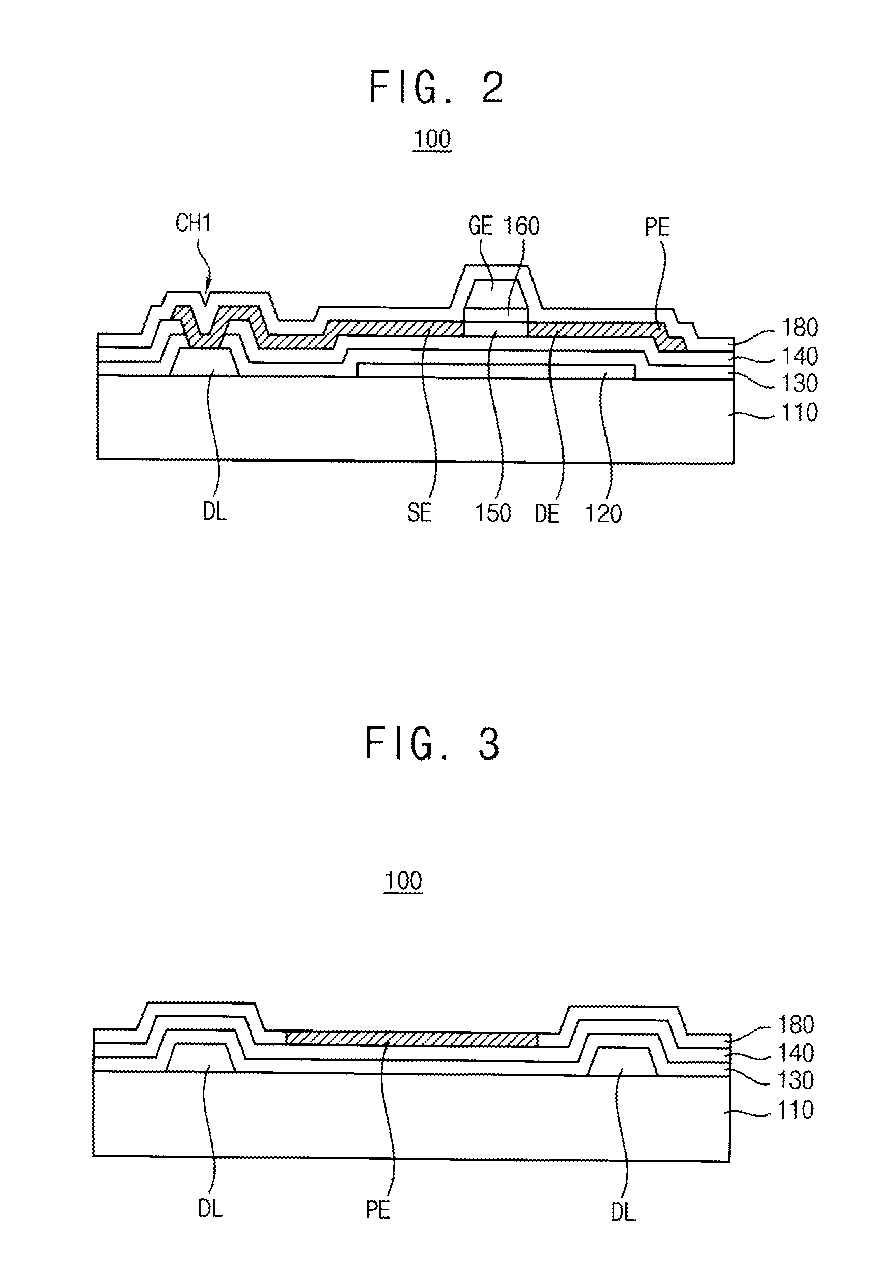
[0034]Hereinafter, example embodiments of the present invention will be explained in detail with reference to the accompanying drawings. Although the terms first, second, etc. may be used herein to describe various signals, elements, components, regions, layers, and / or sections, these signals, elements, components, regions, layers, and / or sections should not be limited by these terms. These terms may be used to distinguish one signal, element, component, region, layer, or section from another signal, region, layer or section. Thus, a first signal, element, component, region, layer, or section discussed below may be termed a second signal, element, component, region, layer, or section without departing from the teachings of the present invention. The description of an element as a “first” element may not require or imply the presence of a second element or other elements. The terms first, second, etc. may also be used herein to differentiate different categories of elements. For conc...


PUM


Abstract

A thin film transistor substrate includes the following elements: a base substrate, a data line disposed on the base substrate, a source electrode contacting the data line, a drain electrode spaced from the source electrode, a channel disposed between the source electrode and the drain electrode, a pixel electrode electrically connected to the drain electrode, a gate insulation pattern disposed on the channel, and a gate electrode disposed on the gate insulation pattern.

Description

PRIORITY STATEMENT[0001]This application claims benefit of and priority under 35 U.S.C. §119 to Korean Patent Application No. 10-2012-0133875, filed on Nov. 23, 2012 in the Korean Intellectual Property Office (KIPO), the contents of which are incorporated herein by reference.BACKGROUND[0002]1. Field of the Invention[0003]The present invention is related to thin-film transistor substrate and a method of manufacturing the thin-film transistor substrate. The thin-film transistor substrate may be used in one or more of a display apparatus, a circuit substrate, a semiconductor, etc.[0004]2. Description of the Related Art[0005]Generally, a thin film transistor for controlling a pixel in a display apparatus includes a gate electrode, a source electrode, a drain electrode, and an active pattern forming a channel between the source electrode and the drain electrode. The active pattern includes a channel layer including amorphous silicon, poly silicon, or an oxide semiconductor.[0006]Conventi...

Claims


Application Information

Patent Timeline
Patent Type & Authority Applications(United States)
IPC IPC(8): H01L33/08
CPCH01L27/1222H01L27/1225H01L27/124H01L29/7869H01L29/78696H01L29/41733
Inventor LEE, JI-SEONKIM, DONG-JOKHANG, YOON-HOLEE, YONG-SULEE, JONG-CHAN
Owner SAMSUNG DISPLAY CO LTD
Why Eureka
Try Eureka