Eureka AIR delivers breakthrough ideas for toughest innovation challenges, trusted by R&D personnel around the world.

Image-sensing apparatus

a technology of image sensor and optical filter, which is applied in the direction of instruments, instruments for comonautical navigation, distance measurement, etc., can solve the problems of not having a material or method suitable and effective for forming a two-band pass filter array, and not having a suitable optical filter that can meet the above requirements

Active Publication Date: 2014-05-22
VISERA TECH CO LTD
View PDF6 Cites 47 Cited by
  • Summary
  • Abstract
  • Description
  • Claims
  • Application Information

AI Technical Summary

Benefits of technology

The patent text explains the importance of color image sensors in optoelectronic devices. These sensors convert detected light into electrical signals, and they are commonly used in devices like cameras and smartphones. The text highlights the use of complementary metal oxide semiconductor (CMOS) image sensors, which have become the most popular type of color image sensor. These sensors have a photodiode that can detect and store optical signals, allowing them to create images with signal processing. The text also mentions that the photodiode and signal processing device can be manufactured in a single chip using COMS manufacturing techniques. The technical effect of this patent is to explain the importance and manufacturing techniques of color image sensors, which can be used in various optoelectronic devices.

Problems solved by technology

However, there is currently no suitable optical filter that can meet the above requirements.
Thus, there is no suitable and effective material or method for forming a two-band pass filter array which can be fabricated in mass production that permit only the light in the visible light range to pass to each unit pixel of the color image sensor and only the light in the infrared range to pass to each unit pixel of the ToF camera.

Method used


Image

  • Image-sensing apparatus
  • Image-sensing apparatus
  • Image-sensing apparatus

Examples


Embodiment Construction

[0019]The following description is of the best-contemplated mode of carrying out the invention. This description is made for the purpose of illustrating the general principles of the invention and should not be taken in a limiting sense. For example, the formation of a first feature over, above, below, or on a second feature in the description that follows may include embodiments in which the first and second features are formed in direct contact, and may also include embodiments in which additional features may be formed between the first and second features, such that the first and second features may not be in direct contact. The scope of the invention is best determined by reference to the appended claims.

[0020]It will be understood that although the terms first, second, third, etc., may be used herein to describe various elements, components, regions, layers, and / or sections, these elements, components, regions, layers, and / or sections should not be limited by these terms. Thes...


PUM


Abstract

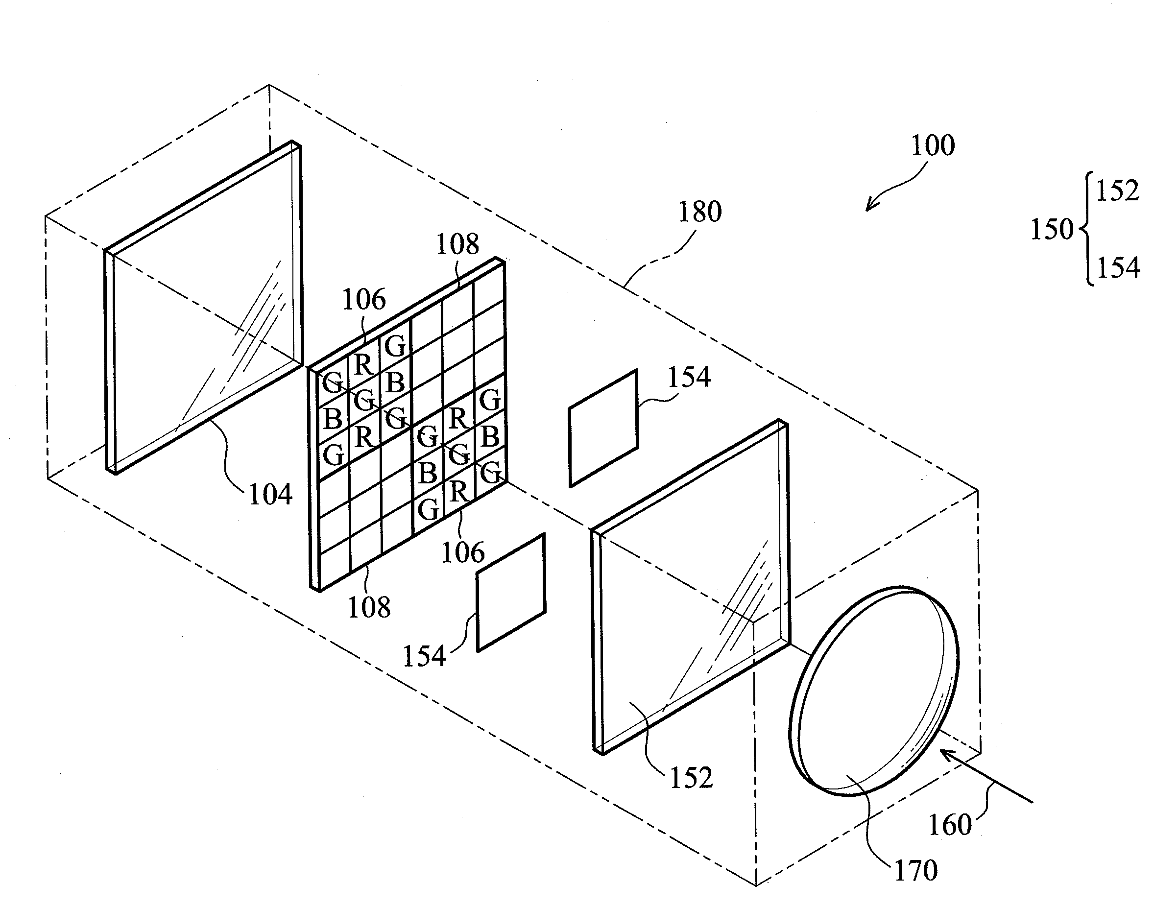
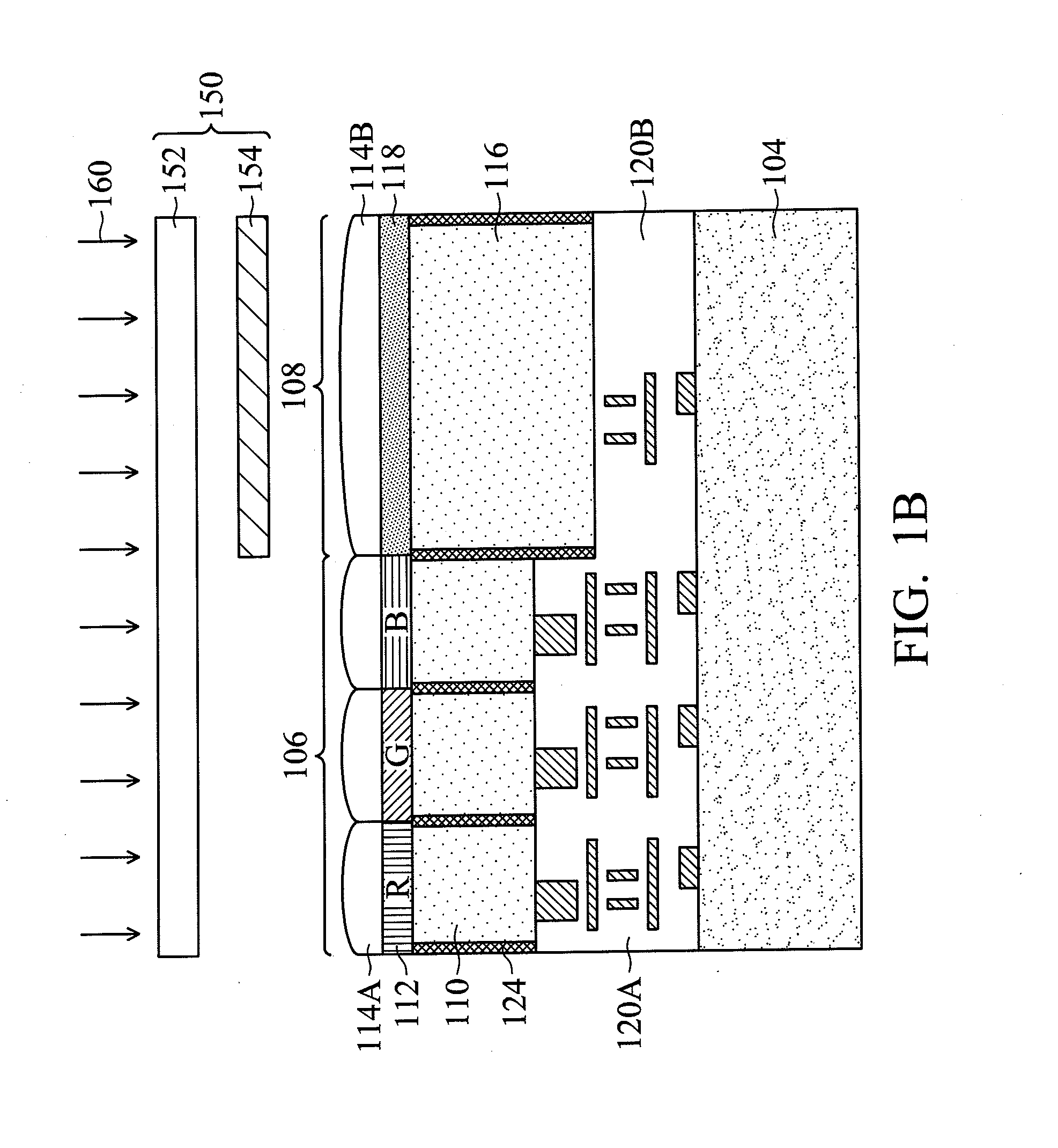
An image-sensing apparatus is provided. The image-sensing apparatus includes: an optical filter array including a two-band passing filter and an infrared filter; an RGB pixel array placed below the two-band passing filter; and a TOF pixel array adjacent to the RGB pixel array and placed below the two-band passing filter and the infrared filter, wherein a combination of the two-band passing filter and the infrared passing filter permits only the incident light in the infrared region to pass to the ToF pixel array.

Description

TECHNICAL FIELD[0001]The present disclosure relates generally to an optoelectronic device, and more particularly to an image-sensing apparatus.BACKGROUND[0002]A color image sensor is a necessary component in many optoelectronic devices. The color image sensor is a photoelectric conversion device that may transform detected light into electrical signals. A conventional image sensor may include a plurality of unit pixels arranged in an array on a semiconductor substrate. Each of the unit pixels may include a photodiode and / or a plurality of transistors. The photodiode may detect external light and / or may generate and store charges, and the transistor may output electrical signals according to the stored charges. A complementary metal oxide semiconductor (CMOS) image sensor is the most commonly used image sensor. The CMOS image sensor may include a photodiode that can receive and / or store optical signals and can realize images with signal processing. The photodiode may be manufactured ...

Claims


Application Information

Patent Timeline
IPC IPC(8): G01J3/51G01C3/08G01S17/86G01S17/894
CPCG01C3/08G01J3/51H01L27/14621H01L27/14629H01L27/1464H01L27/14645H01L27/14649G01S7/4816G01S17/86G01S17/894
Inventor WANG, WEI-KOCHANG, CHIN-CHINGWU, CHIA-HUIHUANG, CHIEN-HSIUNGLIN, CHENG-XUANCHEN, CHANG WEI
Owner VISERA TECH CO LTD
Why Eureka
Eureka Blog
Learn More