Display device, liquid crystal display device, electronic apparatus, and display device manufacturing method

a liquid crystal display and display device technology, applied in the direction of instruments, computing, electric digital data processing, etc., can solve the problems of increasing the thickness of the device itself, affecting the accuracy of touch positions by fingers or pennies, and curved electrical field lines distributed on the transparent conductive film. achieve the effect of low cos

Active Publication Date: 2014-05-15
TIANMA MICRO ELECTRONICS CO LTD
View PDF15 Cites 11 Cited by
  • Summary
  • Abstract
  • Description
  • Claims
  • Application Information

AI Technical Summary

Benefits of technology

The patent aims to provide a display device that can detect touch accurately and at a low cost. The invention is designed to overcome the limitations of existing techniques and provide a thin and small-sized display.

Problems solved by technology

However, when the AC voltages are simply applied to the transparent conductive film from the four corners, an electric field lines distributed on the transparent conductive film becomes curved and non-linear.
Therefore, the touched positions by a finger or a pen cannot be detected accurately.
However, such structure has the touch sensor provided further on the display screen, so that there are some issues to be overcome, e.g., an increase in the thickness of the device itself, an increase in the cost, and deterioration of the display quality by putting the touch sensor on the display.
However, there are still remained issues with the display devices disclosed in Patent Documents 3 and 4 as follows.
Therefore, the display devices disclosed in Patent Documents 3 and 4 are suited for reducing the weight, the size, and the thickness, but not capable of correctly detecting the positions touched by a finger or a pen.
Further, the conductive paste for the linearization patterns is normally made with fine powders of noble metals such as silver, so that such expensive material is required.
As a result, the cost for manufacturing the display devices is increased if the techniques of Patent Documents 3 and 4 and the technique of Patent Document 2 are simply combined in order to form the linearization patterns on the counter electrode.

Method used


Image

  • Display device, liquid crystal display device, electronic apparatus, and display device manufacturing method
  • Display device, liquid crystal display device, electronic apparatus, and display device manufacturing method
  • Display device, liquid crystal display device, electronic apparatus, and display device manufacturing method

Examples


first exemplary embodiment

(Overall Structure of Display Device)

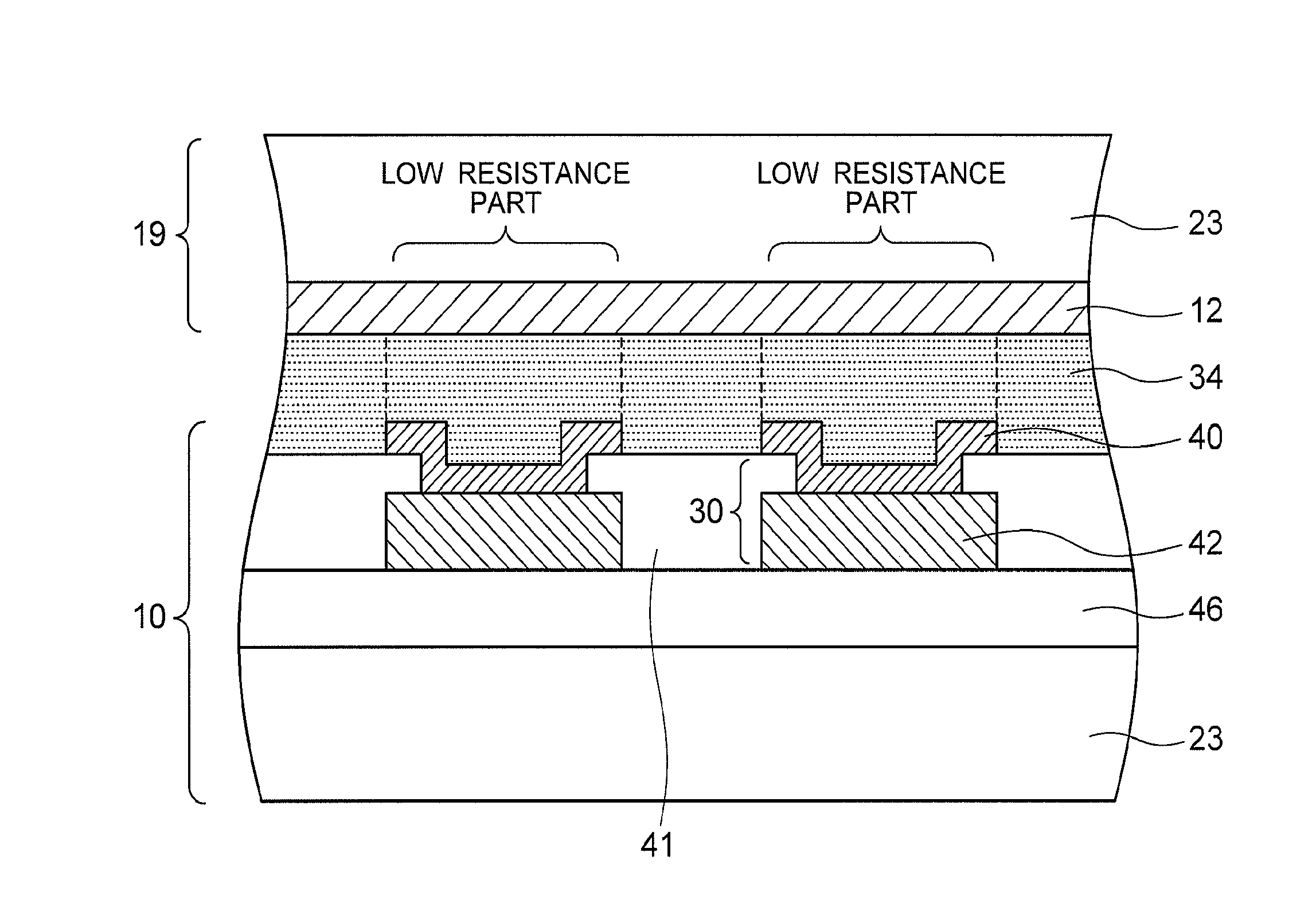
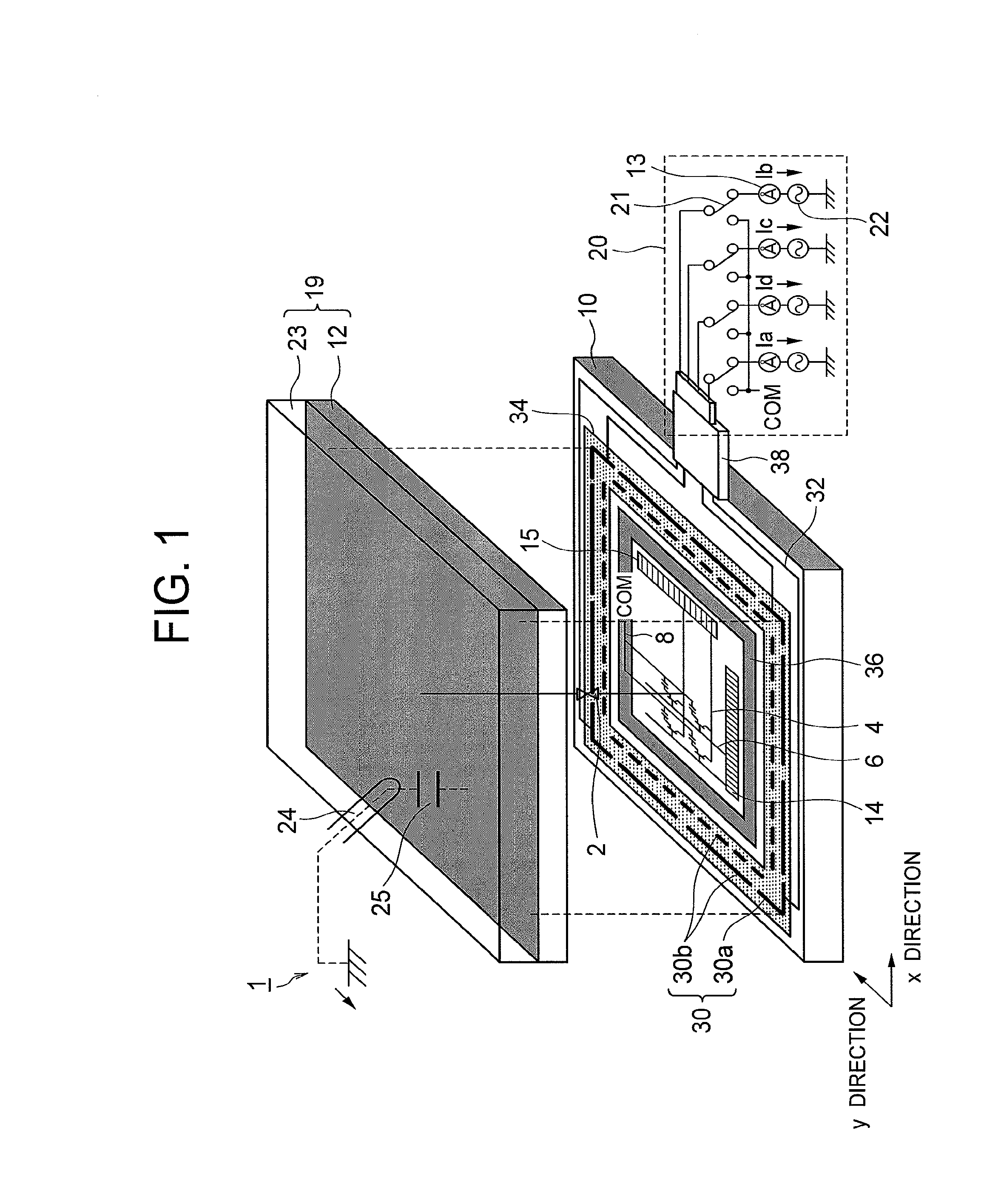
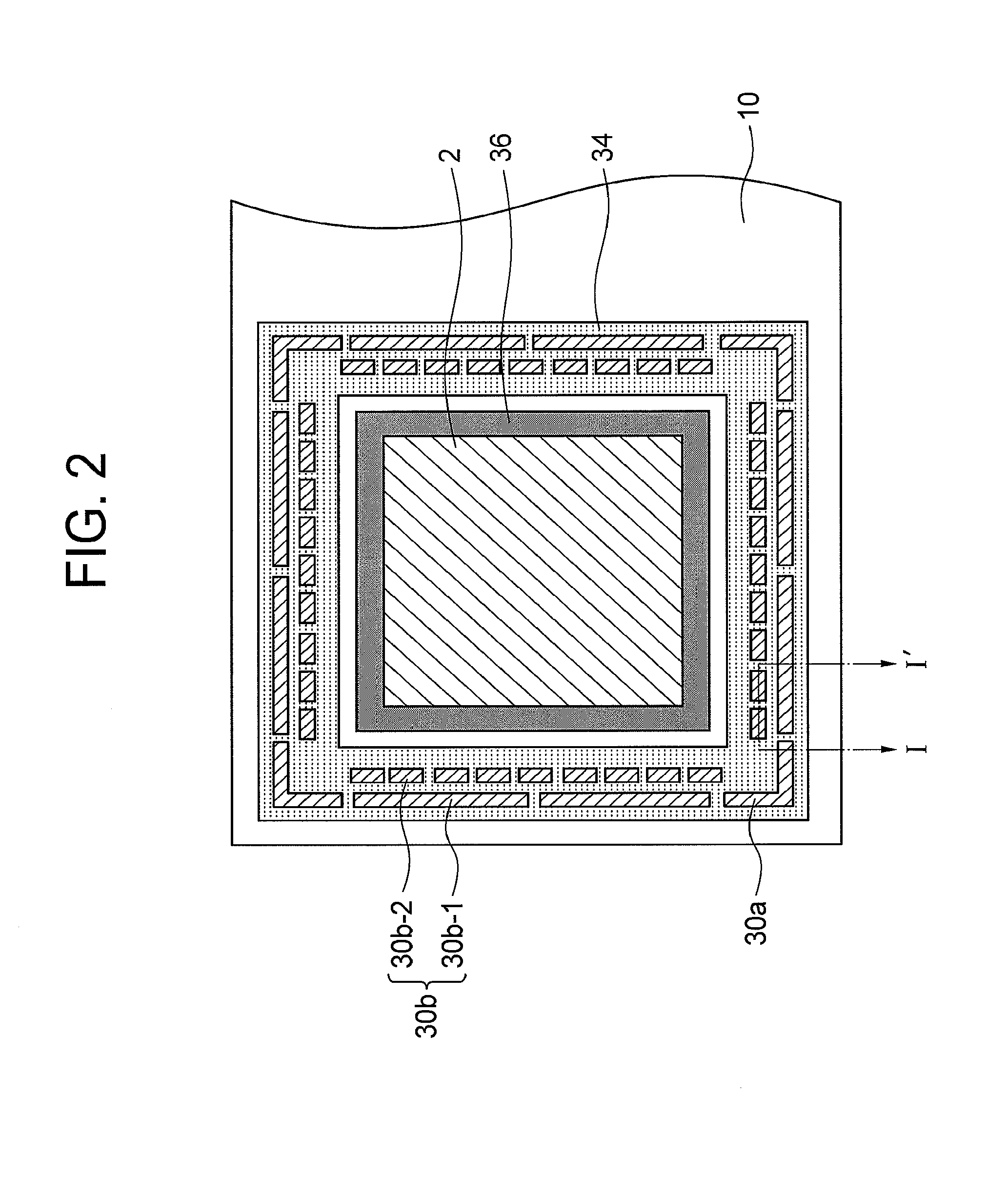
[0058]First, a specific structure of a display device according to this exemplary embodiment will be described in order from the overall structure to the detailed structure of each part. FIG. 1 is a perspective view showing an example of an overall schematic structure, which schematically illustrates a display device with a built-in touch sensor according to a first exemplary embodiment of the invention.

[0059]As shown in FIG. 1, a display device 1 of this exemplary embodiment is a liquid crystal display device (LCD) which includes a touch sensor that is capable of detecting touches of a finger or a pen on a display screen and position coordinates thereof.

[0060]Other than the liquid crystal display device, the display device 1 can also be a display device such as a plasma display device (PDP), an organic EL display device, or the like.

[0061]The display device 1 is configured, including a display device substrate 10, a counter substrate 19, and a p...

second exemplary embodiment

[0158]Next, a second exemplary embodiment of the invention will be described by referring to FIG. 7. Hereinafter, the practically same structural elements as those of the first exemplary embodiment are omitted, and only different points will be described. FIG. 7 is a plan model illustration showing an example of a schematic structure of a display device according the second exemplary embodiment of the invention.

[0159]In the above-described first exemplary embodiment, the anisotropic conductor and the sealing agent are different structural elements. However, the second exemplary embodiment employs a structure where the anisotropic conductor also functions as the sealing agent. That is, it is a case where the conductive member is inserted between the first substrate and the second substrate to function as the sealing agent for sealing the display element.

[0160]Specifically, as shown in FIG. 7, in a display device 200 according to the second exemplary embodiment, linearization pattern ...

third exemplary embodiment

[0166]Next, a third exemplary embodiment of the invention will be described by referring to FIG. 8 and FIG. 9. Hereinafter, the practically same structural elements as those of the first exemplary embodiment are omitted, and only different points will be described. FIG. 8 is a plan model illustration showing an example of a schematic structure which illustrates a relation between linearization pattern sections and an anisotropic conductor of a display device according to the third exemplary embodiment of the invention. FIG. 9 is a fragmentary sectional view showing a II-II′ part of FIG. 8.

[0167]In this exemplary embodiment, the layout pattern of the conductor as an example of the conductive member is formed to correspond to the layout pattern of the linearization pattern sections. That is, it is a case where the conductive member is formed to have a pattern of a plurality of divided sections, and the conductive member pattern has the same layout pattern as that of the linearization ...


PUM

PropertyMeasurementUnit
parasitic capacitanceaaaaaaaaaa
sizeaaaaaaaaaa

Abstract

To provide a low-cost display device which can accurately detect a position touched by a finger. A display device displays an image by having display elements capable of performing electro-optic responses formed between conductible first and second substrates, and detects a contact position touched by a contact body by having a conductive impedance surface formed on the second substrate side. The display device includes: linearization pattern sections formed on the first substrate, which include a plurality of electrodes capable of detecting electric currents on a conductive impedance surface; and a conductive member which electrically connects the linearization pattern sections with the conductive impedance surface on the second substrate.

Description

CROSS-REFERENCE TO RELATED APPLICATION[0001]This application is a Continuation application of U.S. application Ser. No. 12 / 417,255, filed Apr. 2, 2009, which is based upon and claims the benefit of priority from Japanese patent application No. 2008-101967, filed on Apr. 9, 2008, the disclosures of which are incorporated herein in their entirety by reference.BACKGROUND OF THE INVENTION[0002]1. Field of the Invention[0003]The present invention relates to a display device, a liquid crystal display device, an electronic apparatus, and a display device manufacturing method. More specifically, the present invention relates to a display device and the like provided with a touch sensor that is capable of detecting positions touched by a finger or a pen.[0004]2. Description of the Related Art[0005]A touch sensor is a device for detecting positions touched by a finger or a pen, and it is normally used in combination with a display device such as a liquid crystal display device (LCD), a plasma...

Claims


Application Information

Patent Timeline
Patent Type & Authority Applications(United States)
IPC IPC(8): G02F1/1343
CPCG02F1/1343G06F3/0412G06F3/0443G06F3/0445
Inventor YANASE, JIROHAGA, HIROSHI
Owner TIANMA MICRO ELECTRONICS CO LTD
Why Eureka
Try Eureka