
Conductive sheet, touch panel, display device, method for producing said conductive sheet, and non-transitory recording medium

a technology of conductive sheets and display devices, which is applied in the direction of conductive layers on insulating supports, instruments, etc., can solve the problems of generating moiré phenomena (interference patterns), affecting the user's experience, etc., to achieve easy detection and easy noise of graininess or roughness

Active Publication Date: 2014-04-24
FUJIFILM CORP
View PDF4 Cites 44 Cited by
  • Summary
  • Abstract
  • Description
  • Claims
  • Application Information

AI Technical Summary

Benefits of technology

This patent aims to improve the appearance of touch panels and displays by reducing the roughness or graininess caused by the pattern of the electrode. By using a special conductive sheet and method of producing it, the amount of light transmitted through the electrode is minimized, resulting in a smoother and more transparent appearance. In addition, the patent provides a non-transitory recording medium for this new technology.

Problems solved by technology

As a result, a problem arises in that the transmission speed of current between the electrodes becomes slower, such that the time (i.e., response speed) required to detect the contact position after the touch panel has been touched is delayed.
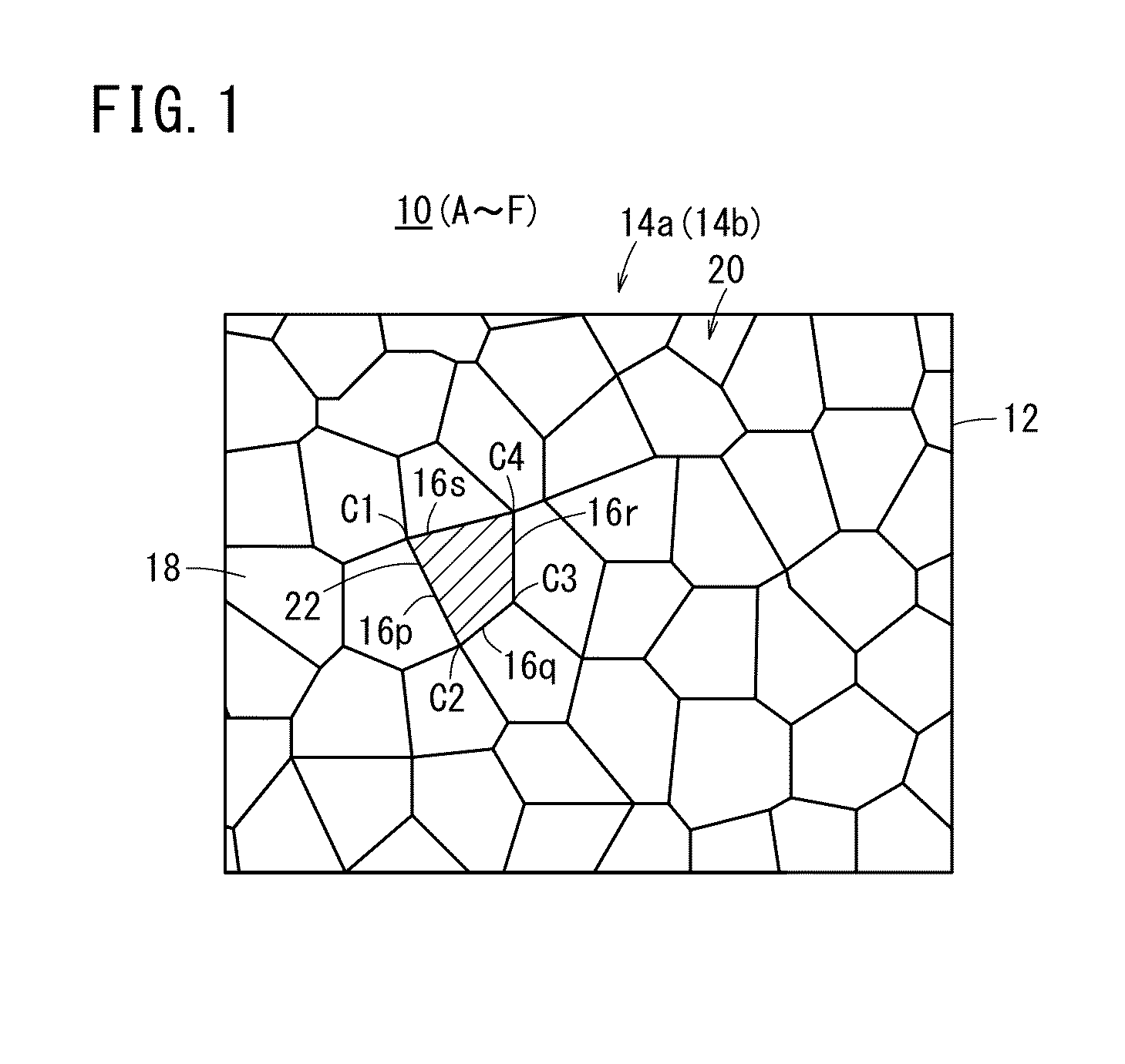
For example, if the same mesh patterns are regularly arranged in a uniform manner, there is a disadvantage that, in relation to pixels constituting the display screen, moiré phenomena (interference patterns) are generated easily.

Method used


Image

  • Conductive sheet, touch panel, display device, method for producing said conductive sheet, and non-transitory recording medium
  • Conductive sheet, touch panel, display device, method for producing said conductive sheet, and non-transitory recording medium
  • Conductive sheet, touch panel, display device, method for producing said conductive sheet, and non-transitory recording medium

Examples


example applied

[Example Applied to Resistive Film Type Touch Panel]

[0411]The present invention can be applied not only to an electrostatic capacitance type, but also to a resistive film type (as well as to a digital type, or an analog type) of touch panel 160. Below, with reference to FIGS. 51 to 53, the structure and operational principles of such a touch panel 160 will be described.

[0412]A digital resistive film type touch panel 160 comprises a lower side panel 162, an upper side panel 164 arranged in confronting relation to the lower side panel 162, a frame adhesive layer 166 bonded to peripheral edge portions of the lower side panel 162 and the upper side panel 164, and which serves to electrically insulate both the panels from each other, and an FPC 168 (Flexible Printed Circuit) sandwiched between the lower side panel 162 and the upper side panel 164.

[0413]As shown in FIG. 51 and FIG. 52A, the upper side panel 164 includes a first transparent substrate 170a made from a flexible material (e.g...

##ventive example 1

Inventive Example 1

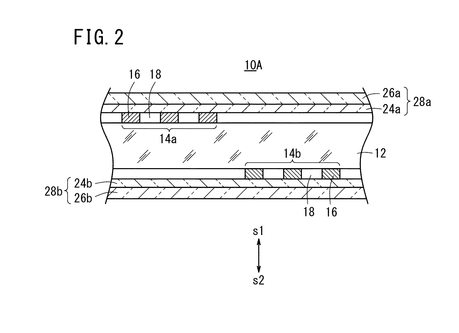
[0490]A conductive sheet 10 according to the first inventive example was manufactured using polychlorotrifluoroethylene (PCTFE) with an index of refraction n1=1.42 as the first protective layer 26a. In this case, the relative index of refraction nr1 was nr1=(1.42 / 1.64)=0.86.

##ventive example 2

Inventive Example 2, Comparative Examples 1 to 3

[0491]A conductive sheet 10 according to the second inventive example was manufactured using polymethyl methacrylate (PMMA) with an index of refraction n1=1.50 as the first protective layer 26a. In this case, the relative index of refraction nr1 was nr1=(1.50 / 1.64)=0.91.

[0492]Further, concerning comparative example 1 corresponding to the pattern PT1 (see FIG. 57A), comparative example 2 corresponding to the pattern PT2 (see FIG. 57B), and comparative example 3 corresponding to the pattern PT3 (see FIG. 57C), respective samples were made by covering the aforementioned patterns with polymethyl methacrylate.

Inventive Example 3, Inventive Example 7

[0493]Conductive sheets 10 according to the third and seventh inventive examples were manufactured using polystyrene (PS) with an index of refraction n1=1.60 as the first protective layer 26a. In this case, the relative index of refraction nr1 was nr1=(1.60 / 1.64)=0.97.


PUM

PropertyMeasurementUnit
Fractionaaaaaaaaaa
Fractionaaaaaaaaaa
Angleaaaaaaaaaa

Abstract

The present invention pertains to: a conductive sheet, a touch panel, a display device, a method for producing the conductive sheet, and a recording medium. In the present invention, the relative refractive index of a substrate with respect to a first protective layer, and / or the relative refractive index of the substrate with respect to a second protective layer is 0.86-1.15. The relative refractive index of a first substrate with respect to the first protective layer, and / or the relative refractive index of a second substrate with respect to the second protective layer is 0.86-1.15.

Description

CROSS-REFERENCE TO RELATED APPLICATIONS AND PRIORITY CLAIMS[0001]This application is a Continuation of International Application No. PCT / JP2012 / 067620 filed on Jul. 10, 2012, which was published under PCT Article 21(2) in Japanese, which is based upon and claims the benefit of priority from Japanese Patent Applications No. 2011-152534 filed on Jul. 11, 2011, No. 2011-152759 filed on Jul. 11, 2011, No. 2011-193505 filed on Sep. 6, 2011, and No. 2011-193506 filed on Sep. 6, 2011, the contents all of which are incorporated herein by reference.TECHNICAL FIELD[0002]The present invention relates to a conductive sheet, a touch panel and a display device, a method for producing the conductive sheet, and a non-transitory recording medium.BACKGROUND ART[0003]Recently, electronic devices that incorporate touch panels therein have been spreading widely. Touch panels are mounted in many devices including small screen, such as portable phones, PDAs (Personal Digital Assistants), or the like. In t...

Claims


Application Information

Patent Timeline
IPC IPC(8): H05K1/02G06F1/16B32B7/023
CPCG06F1/1692H05K1/0298B32B15/02G06F2203/04103G06F2203/04111B32B15/08B32B27/302B32B27/32B32B27/40B32B2307/202B32B2307/412B32B2307/418B32B2457/208G06F3/0446G06F3/0445B32B7/023G06F3/041H01B5/14G06F3/044
Inventor IWAMI, KAZUCHIKAISHIBASHI, HIDEYASUWAKUI, TAKASHI
Owner FUJIFILM CORP
Learn More