Semiconductor package, method and mold for producing same, input and output terminals of semiconductor package

a semiconductor and packaging technology, applied in semiconductor devices, semiconductor/solid-state device details, electrical devices, etc., can solve the problems of low design flexibility, low input/output impedance of semiconductor elements, low permittivity of encapsulation resin, etc., and achieve excellent high frequency characteristics

Active Publication Date: 2014-03-20
PANASONIC SEMICON SOLUTIONS CO LTD
View PDF2 Cites 13 Cited by
  • Summary
  • Abstract
  • Description
  • Claims
  • Application Information

AI Technical Summary

Benefits of technology

[0014]According to the present invention, in a resin-encapsulated package, an electric conductor for ground enhancement can be firmly grounded, and furthermore the phase advance relative to a ground surface can also be reduced. Thus, an inexpensive semiconductor package having excellent high frequency characteristics can be provided on which a high-frequency, high-power semiconductor element is mounted.

Problems solved by technology

However, an encapsulation resin has low permittivity, and thus flexibility is low in designing characteristic impedance of lead terminals through which a high frequency signal is input to and output from a semiconductor element.
In particular, since a high-power semiconductor element has a large chip size, the input / output impedance of the semiconductor element itself is low, and a mismatch is likely to occur between the input / output impedance and the impedance of a load circuit including characteristic impedance of a lead terminal of a package.

Method used


Image

  • Semiconductor package, method and mold for producing same, input and output terminals of semiconductor package
  • Semiconductor package, method and mold for producing same, input and output terminals of semiconductor package
  • Semiconductor package, method and mold for producing same, input and output terminals of semiconductor package

Examples


embodiment 1

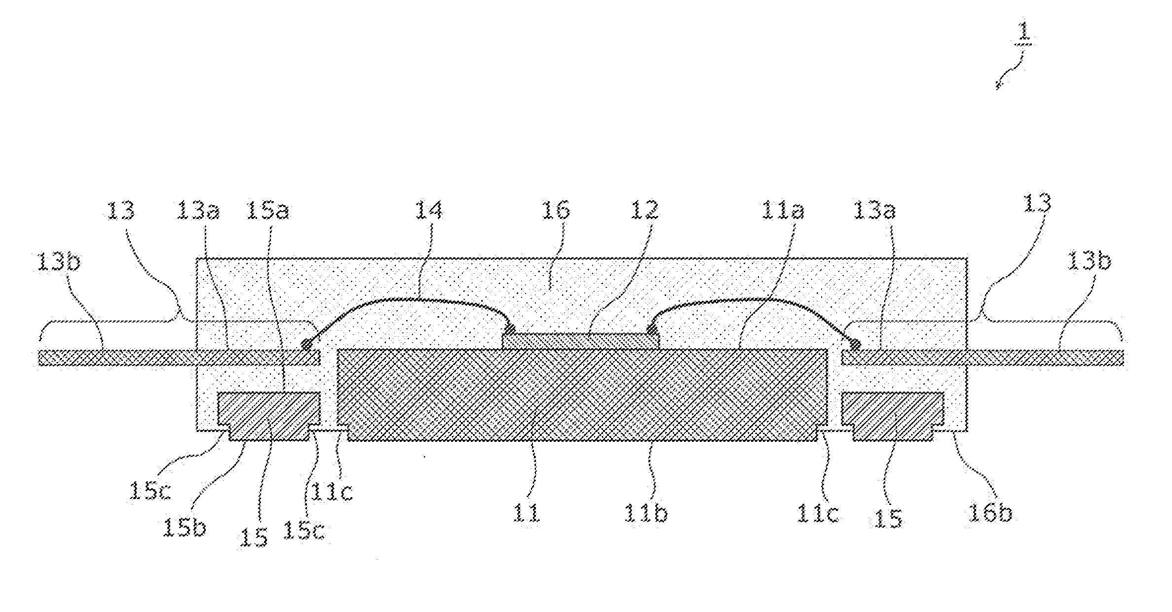
[0077]FIG. 1 is a cross-sectional view illustrating a structure of a semiconductor package according to Embodiment 1 of the present invention. A semiconductor package 1 illustrated in the drawing is a resin-encapsulated package, and includes: a die pad 11; a semiconductor element 12; plural lead terminals 13; bonding wires 14 which connect the semiconductor element 12 and inner lead portions 13a; ground enhancing metal bodies 15; and an encapsulation resin 16. It should be noted that a portion of each lead terminal 13 located inside the encapsulation resin 16 is referred to as the inner lead portion 13a, and a portion thereof located outside the encapsulation resin is referred to as an outer lead portion 13b.

[0078]The semiconductor element 12 is a high-frequency power amplifying element which is die-bonded onto a main surface 11a of the die pad 11, amplifies power of a high frequency signal input through one of the lead terminals 13, and outputs the high frequency signal whose powe...

embodiment 2

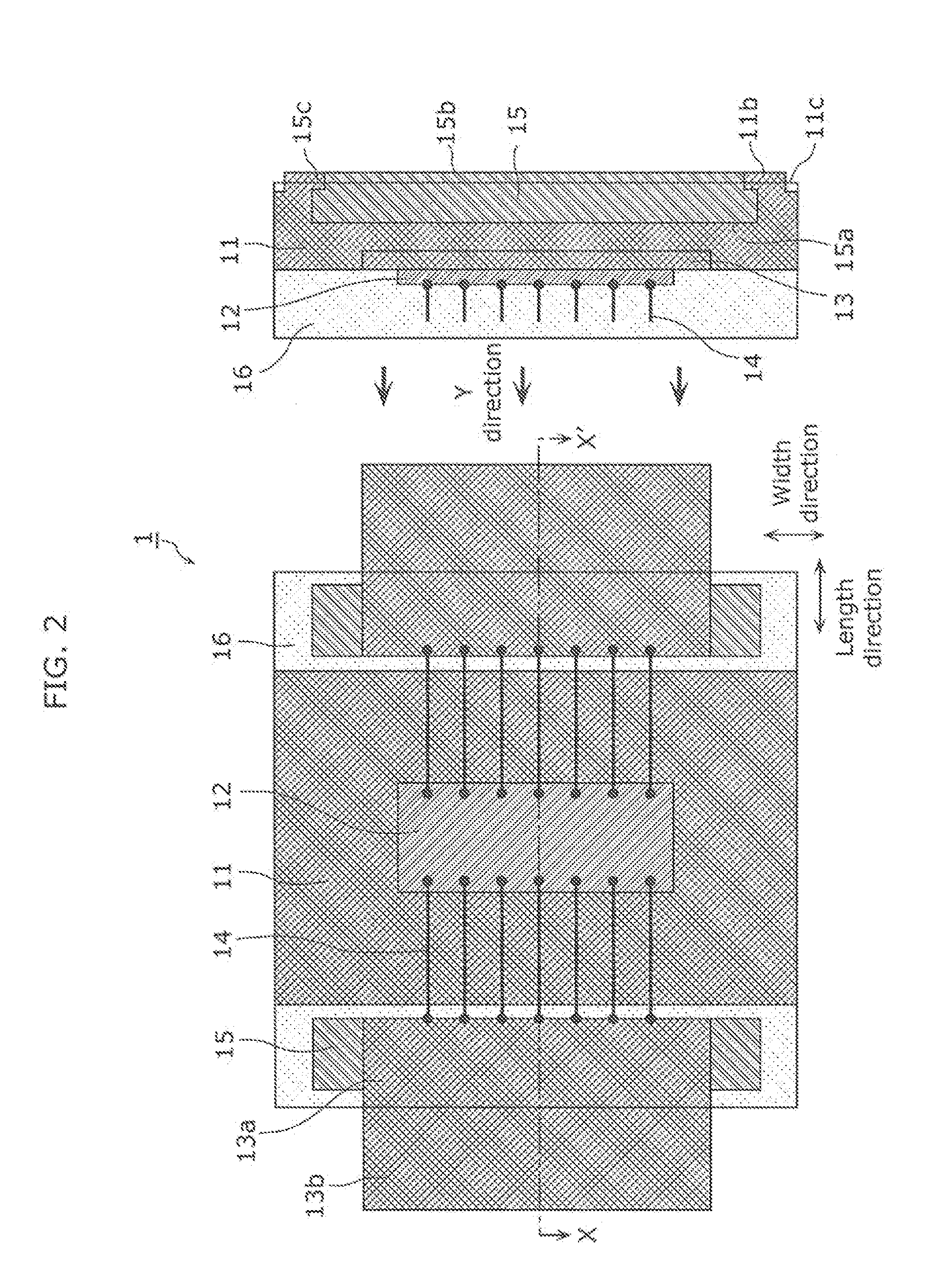
[0110]FIG. 3 is a perspective view of a top surface of a semiconductor package according to Embodiment 2 of the present invention. A semiconductor package 2 illustrated in the drawing is a resin-encapsulated package, and includes a die pad 21, a semiconductor element 12, plural lead terminals 13, bonding wires 14, a ground enhancing metal body 15, and an encapsulation resin 16. Compared with the semiconductor package 1 according to Embodiment 1, the semiconductor package 2 according to the present embodiment is different therefrom in the following points: the die pad 21 has a greater width than the encapsulation resin 16, and cutouts 11d for screwing are provided in the areas of the die pad 21 projecting from the encapsulation resin 16 in the width direction. A description of the same points as the semiconductor package 1 according to Embodiment 1 is omitted, and the following describes only points different from the semiconductor package 1.

[0111]The die pad 21 is a flat plate inclu...

embodiment 3

[0115]In the present embodiment, a description is given of a method for fabricating a semiconductor package according to the present invention.

[0116]FIG. 4 is a flow chart of a production process for a lead frame for fabricating the semiconductor package according to the present invention. Further, FIG. 5 illustrates a process flow of fabricating the semiconductor package according to the present invention from the lead frame. In the method for fabricating the semiconductor package according to the present invention, steps (a) to (c) of FIG. 4 are executed, and thereafter steps (a) to (d) of FIG. 5 are executed. Specifically, (a) to (c) of FIG. 4 show a fabricating process for the lead frame from which the die pads 11 and the lead terminals 13 included in the semiconductor package 1 according to Embodiment 1 are obtained. Furthermore, (a) and (b) of FIG. 5 show steps of mounting elements onto the lead frame, (c) of FIG. 5 shows an encapsulation step using the encapsulation resin 16,...


PUM


Abstract

A semiconductor package according to the present invention includes: a semiconductor element where a high frequency signal is input or output; a planar lead terminal having an end electrically connected to an input terminal or an output terminal of the semiconductor element; an encapsulation resin for encapsulating the lead terminal and the semiconductor element, the lead terminal having another end exposed from the resin; and a ground enhancing metal body encapsulated in the encapsulation resin, having a first main surface facing the lead terminal and a second main surface exposed from the encapsulation resin, wherein the ground enhancing metal body has a shape with a cross section parallel to the second main surface and having a smaller area than an area of the first main surface.

Description

TECHNICAL FIELD[0001]The present invention relates to a semiconductor package, a method and a mold for fabricating the same, and input and output terminals of the semiconductor package, and in particular to a resin-encapsulated semiconductor package for a high frequency semiconductor device which outputs a high frequency signal at a high level.BACKGROUND ART[0002]Resin-encapsulated packages can be fabricated in large quantities at a low cost, and thus are most widely used as packages of semiconductor elements for general use.[0003]However, an encapsulation resin has low permittivity, and thus flexibility is low in designing characteristic impedance of lead terminals through which a high frequency signal is input to and output from a semiconductor element. There are few examples in which resign-encapsulated packages are used when a high frequency signal of hundreds of MHz or more is involved. In particular, since a high-power semiconductor element has a large chip size, the input / out...

Claims


Application Information

Patent Timeline
Patent Type & Authority Applications(United States)
IPC IPC(8): H01L23/66H01L23/498H01L21/56H01L23/28
CPCH01L23/66H01L21/56H01L23/498H01L23/28H01L23/3135H01L21/561H01L21/565H01L24/97H01L2224/32245H01L2224/48247H01L2224/49175H01L2224/73265H01L2224/97H01L2924/13091H01L2924/3011H01L23/4334H01L23/562H01L23/49568H01L23/3107H01L2223/6627H01L2924/1306H01L2924/1305H01L2924/13062H01L2924/15747H01L2924/181H01L24/73H01L2924/00012H01L2224/85H01L2924/00
Inventor UNO, TAKASHIIKEDA, HIKARUYAHATA, KAZUHIROIWATA, MOTOYOSHINAITOU, HIROSHIKAMIYAMA, TOMOHIDE
Owner PANASONIC SEMICON SOLUTIONS CO LTD
Why Eureka
Try Eureka