
Semiconductor device with buried bit line and method for fabricating the same

a technology of buried bit lines and semiconductor devices, which is applied in semiconductor devices, diodes, electrical apparatus, etc., can solve the problems of reducing the parasitic capacitance the physical limit of the fabrication technology of mosfet, and the limitation of the parasitic capacitance reduction between adjacent buried bit lines, so as to prevent the body line from being leaned and reduce the parasitic capacitance

Active Publication Date: 2014-03-06
SK HYNIX INC
View PDF4 Cites 6 Cited by
  • Summary
  • Abstract
  • Description
  • Claims
  • Application Information

AI Technical Summary

Benefits of technology

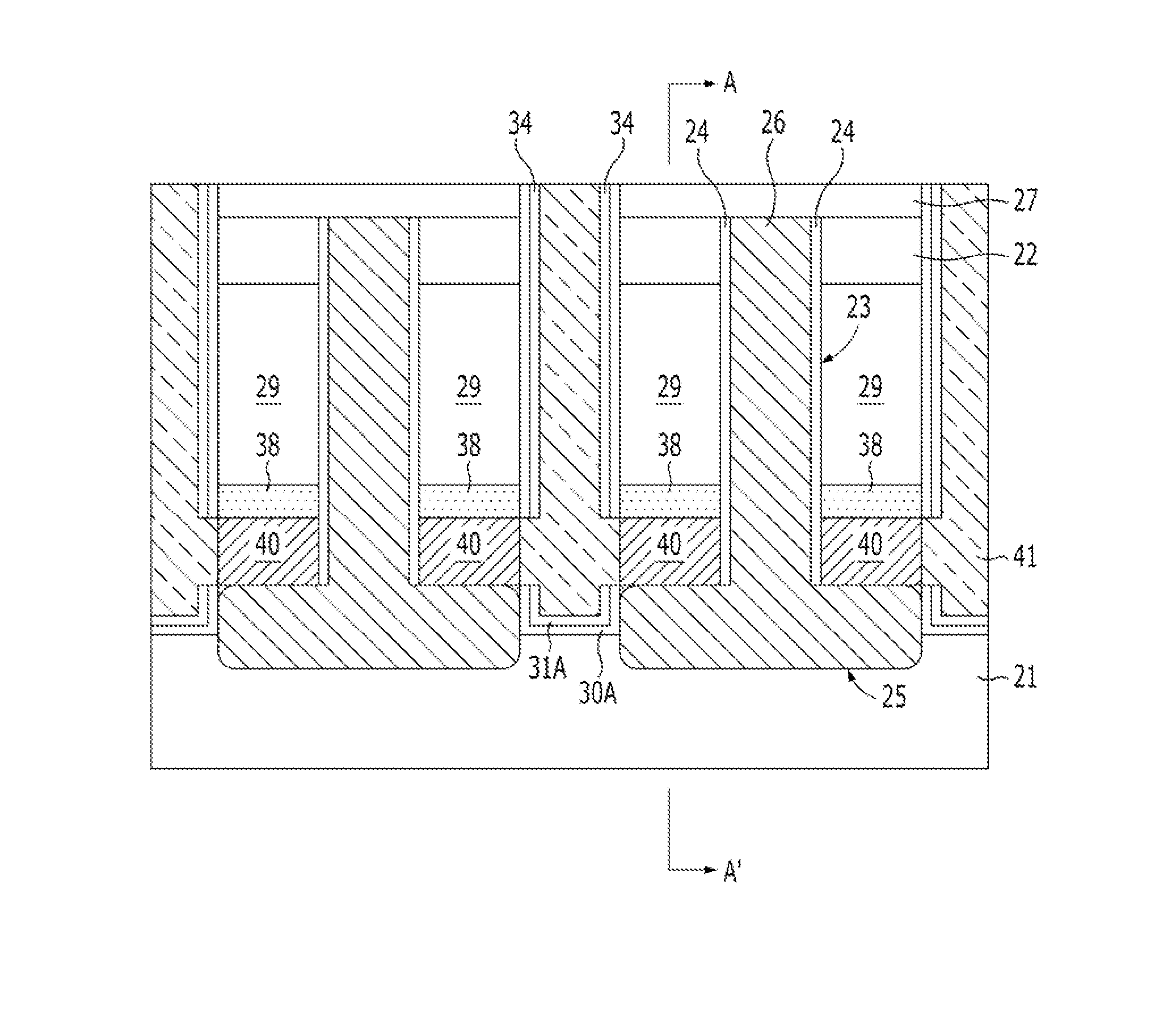
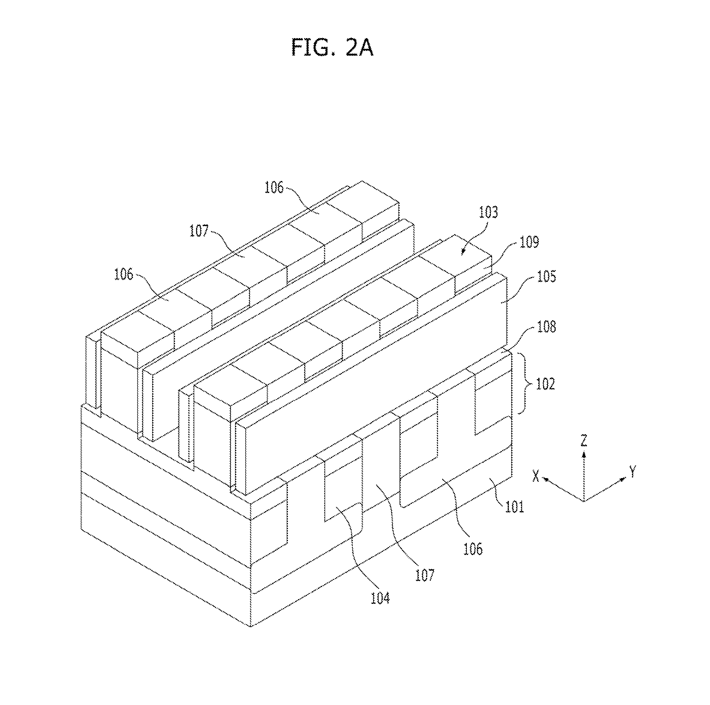
This patent is about a way to make semiconductor devices that don't have problems with pattern leaning, punch-through between rows of bit lines, and reduced parasitic capacitance. The method involves using a supporter to keep the device upright and forming body lines by bisecting the active region to prevent pattern leaning. An insulation material is also used to prevent punch-through between buried bit lines and reduce parasitic capacitance between them. Overall, this method allows for better quality semiconductor devices.

Problems solved by technology

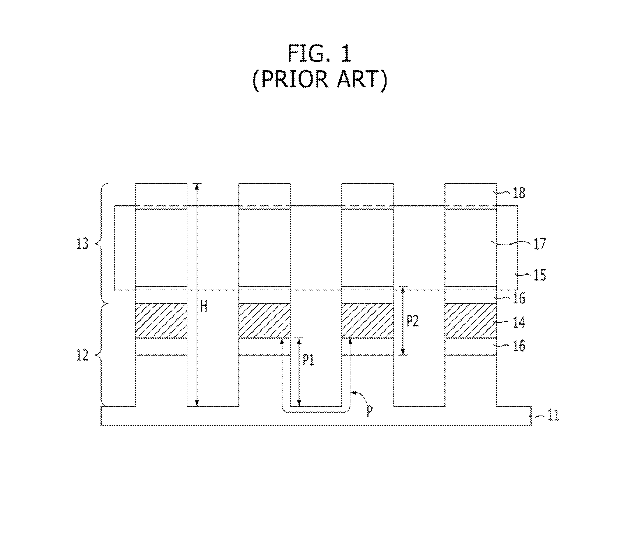
Since it is necessary to continuously improve the degree of integration and performance of a memory device, a fabrication technology of the MOSFET has reached a physical limit.
When the channel length of the MOSFET is reduced, the characteristics of the memory device are degraded due to various problems such as degradation of data retention characteristics.
In addition, in the conventional art, an interval between the adjacent buried bit lines 14 is increased, but there is a limitation in reducing parasitic capacitance between the adjacent buried bit lines 14.

Method used


Image

  • Semiconductor device with buried bit line and method for fabricating the same
  • Semiconductor device with buried bit line and method for fabricating the same
  • Semiconductor device with buried bit line and method for fabricating the same

Examples


Embodiment Construction

[0030]Exemplary embodiments of the present invention will be described below in more detail with reference to the accompanying drawings. The present invention may, however, be embodied in different forms and should not be construed as limited to the embodiments set forth herein. Rather, these embodiments are provided so that this disclosure will be thorough and complete, and will fully convey the scope of the present invention to those skilled in the art. Throughout the disclosure, like reference numerals refer to like parts throughout the various figures and embodiments of the present invention.

[0031]The drawings are not necessarily to scale and in some instances, proportions may have been exaggerated in order to clearly illustrate features of the embodiments. When a first layer is referred to as being “on” a second layer or “on” a substrate, it not only refers to a case where the first layer is formed directly on the second layer or the substrate but also a case where a third laye...


PUM


Abstract

A method for fabricating a semiconductor device includes etching a semiconductor substrate to form bulb-type trenches that define a plurality of active regions in the semiconductor substrate; forming a supporter in each of the bulb-type trenches; dividing each active region, of the plurality of active regions, into a pair of body lines by forming a trench through each active region; and forming a bit line in each body line of the pair of body lines.

Description

CROSS-REFERENCE TO RELATED APPLICATIONS[0001]The present application claims priority of Korean Patent Application No. 10-2012-0094460, filed on Aug. 28, 2012, which is incorporated herein by reference in its entirety.BACKGROUND[0002]1. Field[0003]Exemplary embodiments of the present invention relate to a semiconductor device, and more particularly, to a semiconductor device with a buried bit line and a method for fabricating the same.[0004]2. Description of the Related Art[0005]Most semiconductor devices include transistors. For example, in a memory device such as a DRAM, a memory cell includes a cell transistor such as a MOSFET. In general, in the MOSFET, source / drain regions are formed in a semiconductor substrate, so that a planar channel is formed between the source region and the drain region. Such a general MOSFET is called a ‘planar channel transistor’.[0006]Since it is necessary to continuously improve the degree of integration and performance of a memory device, a fabricati...

Claims


Application Information

Patent Timeline
Patent Type & Authority Applications(United States)
IPC IPC(8): H01L27/06H01L21/8239H10B12/00H10B99/00
CPCH01L21/8239H01L27/0629H01L29/41741H01L29/66666H01L29/7827H01L29/456H10B12/053H10B12/482H10B12/0383H10B12/315
Inventor CHO, HEUNG-JAEHWANG, EUI-SEONGPARK, EUN-SHIL
Owner SK HYNIX INC
Learn More