
Method for producing more particularly processing or populating, a circuit board element and carrier for use in such a method

Inactive Publication Date: 2014-01-09
AT & S AUSTRIA TECH & SYSTTECHN AKTIENGES
View PDF5 Cites 2 Cited by
  • Summary
  • Abstract
  • Description
  • Claims
  • Application Information

AI Technical Summary

Benefits of technology

The present invention aims to provide a method and carrier for carrying out processing or loading of circuit board elements or circuit boards. The invention aims to improve the prior art methods by minimizing or eliminating the use of additional material for frame or carrier elements and simplifying the process of separating the produced or finished circuit board elements from such frame or carrier elements. This will result in a more efficient and cost-effective production process.

Problems solved by technology

Such an edge or peripheral region, which is not required for the functioning of the circuit board, will however, result in elevated costs of such a circuit board, bearing in mind the usually multilayer assembly of expensive materials.
In the context of known production methods of circuit boards, it is, moreover, to be anticipated that regions or areas located between individual circuit board elements, of the common plate-shaped element are discarded as waste products such that elevated costs for the production of circuit boards or circuit board elements will also occur in this respect.
Those known methods for inserting circuit boards into a frame element each completely surrounding the circuit boards in order to produce a composite structure to be jointly handled, in particular, involve the drawbacks that the reception openings to be provided in the frame element for the arrangement of the circuit boards have to be precisely adapted to the dimensions of the circuit boards to be inserted, and a proper fixation, for instance by gluing to the peripheral edges of the circuit boards and frame elements, which usually have comparatively small thicknesses, is therefore extremely difficult and cumbersome.
The known methods, moreover, involve the disadvantages that, in particular, when adapting the dimensions of the circuit boards and / or circuit board elements to be inserted and subsequently treated or processed, also the dimensions of the frame or carrier elements are accordingly differently selected such that in subsequent processing operations, for instance in insertion or loading lines, an exchange of the circuit boards to be treated or processed will require accordingly much time for the conversion of such processing lines to adapt the same to different dimensions of, in particular, the composite structures formed by the at least one frame or carrier element and the plurality of circuit boards.
All of the known methods using frame or carrier elements involve the disadvantage of requiring additional material for such frame or carrier elements, which will be disposed of after having completed the circuit board elements or circuit boards, thus leading to additional costs for the production and, in particular, processing or loading of such circuit board elements.
In addition, the isolation of the circuit board elements or circuit boards after their production or completion by separation from the employed frame or carrier elements will involve accordingly high expenditures.

Method used


Image

  • Method for producing more particularly processing or populating, a circuit board element and carrier for use in such a method
  • Method for producing more particularly processing or populating, a circuit board element and carrier for use in such a method
  • Method for producing more particularly processing or populating, a circuit board element and carrier for use in such a method

Examples


Embodiment Construction

[0043]In the context of the present description, starting materials for a circuit board element to be produced and / or processed are partially also referred to as circuit board elements, since these are mainly semi-finished or intermediate products which, according to the usual nomenclature, are denoted as circuit board elements both before and after processing.

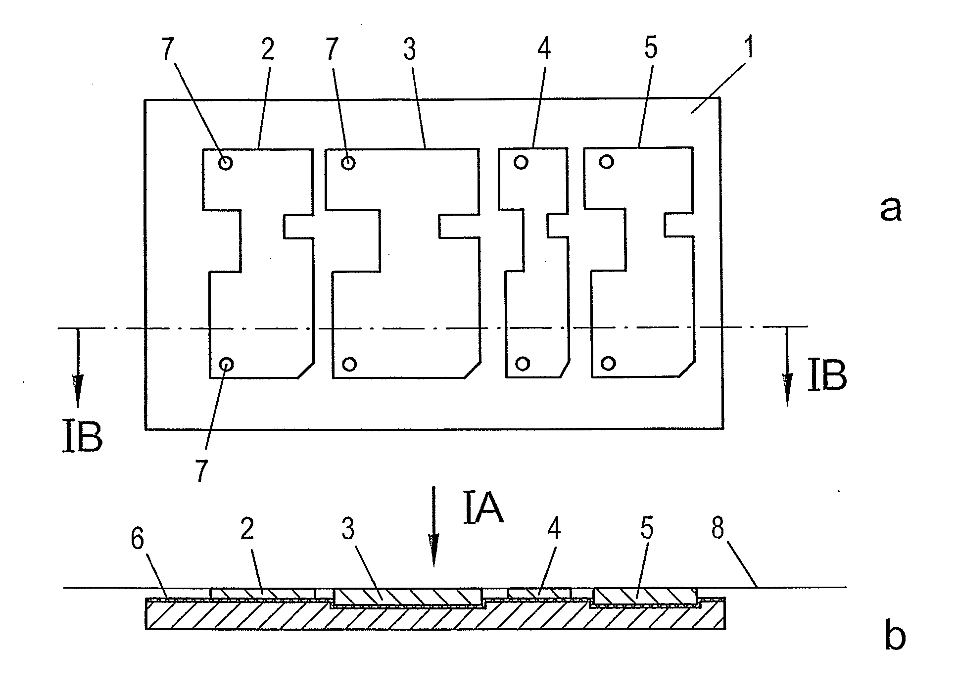
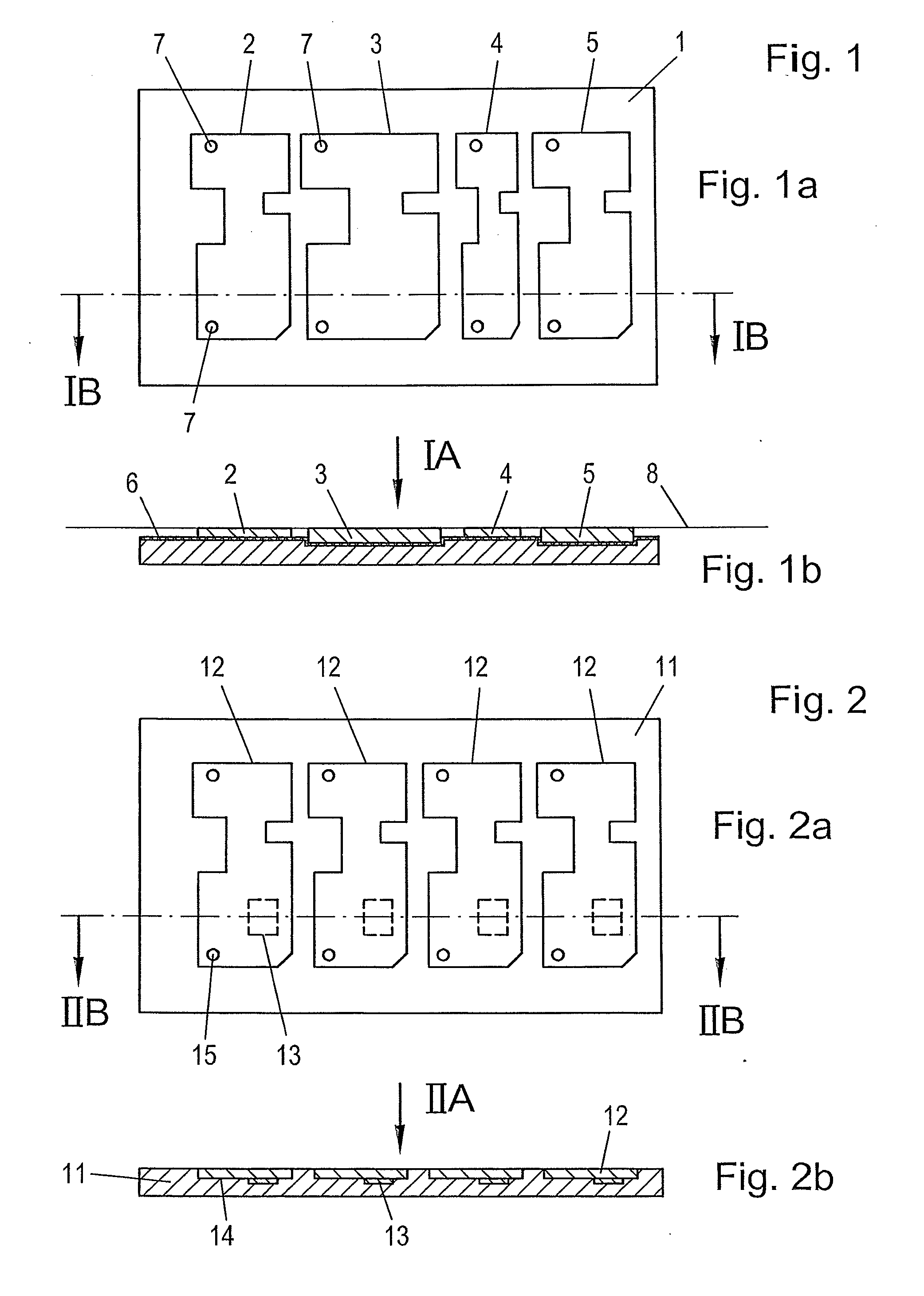
[0044]From the illustration according to FIG. 1, it is apparent that, on a substantially whole-area or full-area carrier generally denoted by 1, a plurality of circuit board elements 2, 3, 4, 5, or starting materials for the same, are disposed and fixed to the carrier 1 via an adhesion layer schematically indicated by 6. In FIG. 1, it is schematically indicated that the circuit board elements 2 to 5 have different sizes and dimensions, with the utilization of space being, in particular, optimized.

[0045]To ensure reliable and precise positioning, it is, moreover, apparent, in particular from FIG. 1a, that the circuit board elem...


PUM

PropertyMeasurementUnit
Temperatureaaaaaaaaaa
Pressureaaaaaaaaaa
Electrical resistanceaaaaaaaaaa

Abstract

In a method for producing a circuit board element, the following steps are provided:providing a substantially whole-area carrier having an adhesive surface;arranging and fixing a starting material of the circuit board element to be produced on the adhesive surface of the carrier;producing the circuit board element fixed on the carrier in a position fixed on the carrier; andremoving the produced circuit board element from the carrier.Furthermore, a carrier for use in such a method is provided, wherein it is possible, in particular, to dispense with complex steps for separating or singulating circuit board elements and, with conservation of resources as a result of reusability of a carrier, it is possible to obtain cost savings in the production of circuit board elements.

Description

[0001]This is a national stage of PCT / AT2012 / 000078 filed Mar. 26, 2012 and published in German, which has a priority of Austria no. GM 177 / 2011, filed Mar. 29, 2011, hereby incorporated by reference.FIELD OF THE INVENTION[0002]The present invention relates to a method for producing, in particular processing or loading a circuit board element, comprising the steps of[0003]providing a substantially full-area carrier having an adhering surface;[0004]disposing and fixing on said adhering surface of the carrier a starting material of the circuit board element to be produced, in particular processed or loaded;[0005]producing, in particular processing or loading, the circuit board element fixed to the carrier in a position fixed on the carrier; and[0006]removing the produced, in particular processed or loaded, circuit board element from the carrier.[0007]The invention relates furthermore to a carrier for usage in such a method, wherein the carrier is formed with an adhering surface for fi...

Claims


Application Information

Patent Timeline
IPC IPC(8): H05K3/00
CPCH05K3/007B22D18/04B22D47/00H05K3/0058H05K3/0097H05K3/30H05K2203/0152Y10T156/17H05K3/36
Inventor FREYDL, GERHARDLEITGEB, MARKUS
Owner AT & S AUSTRIA TECH & SYSTTECHN AKTIENGES
Learn More