Light reflecting member for optical semiconductor, and substrate for mounting optical semiconductor and optical semiconductor device using the light reflecting member
a technology of light reflecting member and optical semiconductor, which is applied in the direction of semiconductor devices, electrical devices, basic electric elements, etc., can solve problems such as sheet deformation, and achieve the effects of accurate shape, reduced cost, and increased light reflection efficiency
- Summary
- Abstract
- Description
- Claims
- Application Information
AI Technical Summary
Benefits of technology
Problems solved by technology
Method used
Image
Examples
example 1
(Thermosetting Resin Composition)
[0096]A thermosetting resin composition for formation of a resin formed body 1 was produced by melt-blending the following materials using a planetary mixer:
[0097]triglycidyl isocyanurate: 100 parts by weight hexahydrophthalic anhydride: 165 parts by weight tetra-n-butylphosphonium-o, o-diethyl phosphorodithioate: 2 parts by weight
[0098]fused silica (average particle diameter: 45 μm): 150 parts by weight rutile-type titanium oxide (average particle diameter: 0.21 μm): 200 parts by weight.
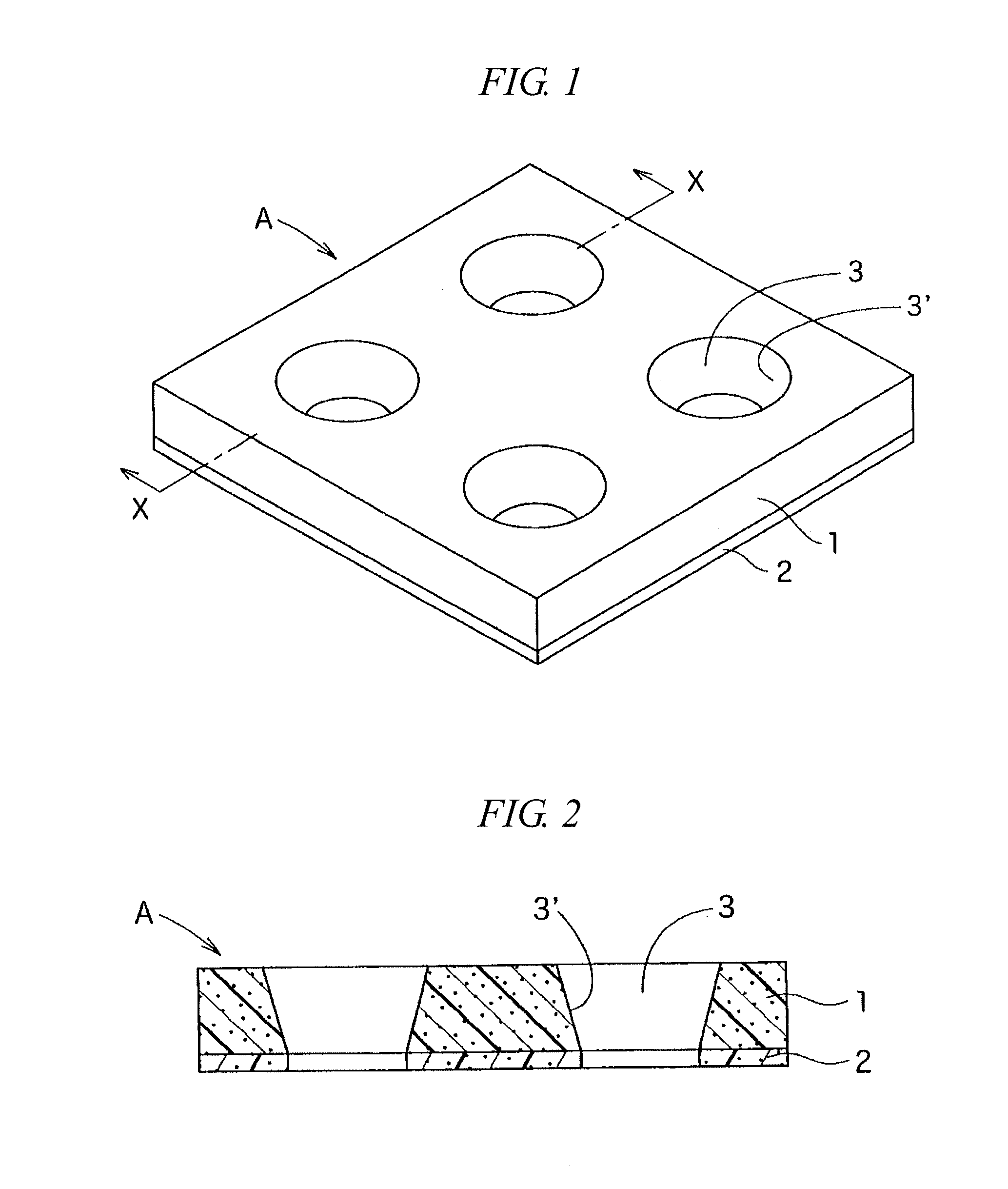
[0099]The above-mentioned thermosetting resin composition was cooled and solidified. The solidified composition was pulverized and then compressed into resin composition tablets. Each resin composition tablet was transfer-molded using a die having a cavity that conforms to the shape of the intended resin formed body 1 shown in FIG. 1 under the following conditions:
[0100]temperature: 180° C.
[0101]clamping pressure: 20 MPa
[0102]injection pressure: 5 MPa
[0103]curing tim...
example 2
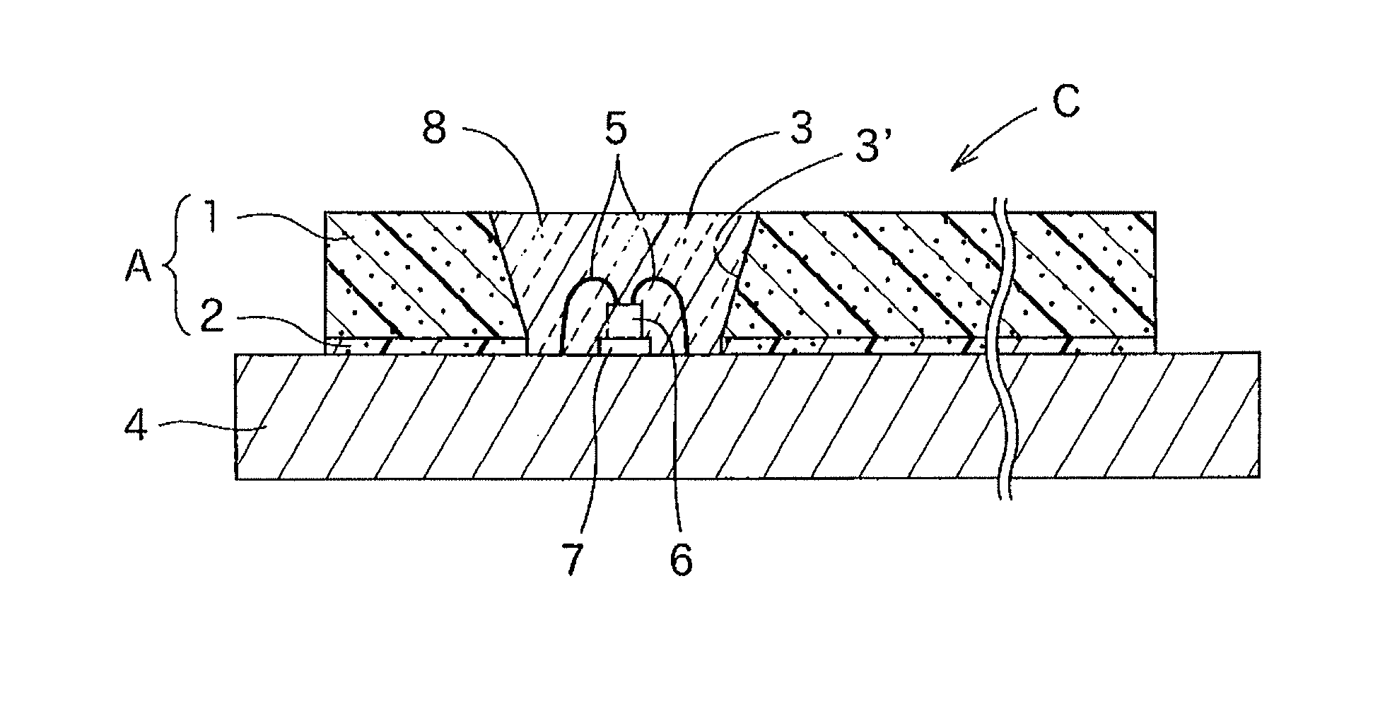
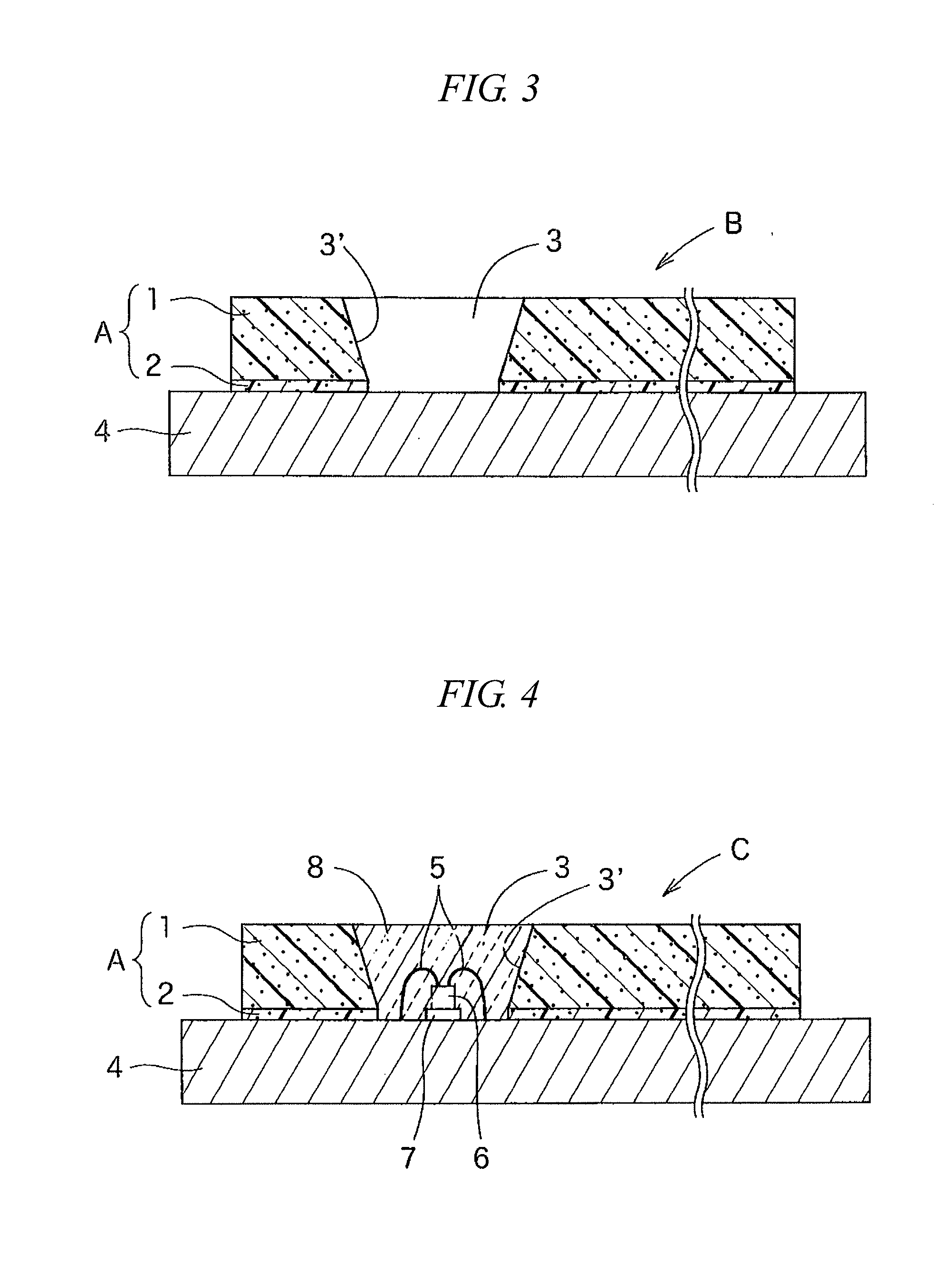
[0110]Optical semiconductor elements (TR-5050 produced by Cree, Inc.) were mounted on the substrate B for mounting an optical semiconductor; that is, they were bonded and fixed to the above-described substrate B at prescribed positions in the openings of the respective through-holes 3 by a die attach agent KER-3000-M2 produced by Shin-Etsu Chemical Co., Ltd.), and wire-bonded to the wiring circuit by gold wires (SR-25 produced by Tanaka Kikinzoku Kogyo K. K.). The recesses formed by the through-holes 3 and the substrate 4 were filled with an encapsulating agent (KER-2500 produced by Shin-Etsu Chemical Co., Ltd.) containing a phosphor (GLD(Y)-550A produced by GeneLite Inc.) at about 10 wt %. Thus, an intended optical semiconductor device C was manufactured (see FIG. 4). Individual optical semiconductor devices corresponding to the respective optical semiconductor elements were produced by cutting the optical semiconductor device C using a blade dicing machine (DFD6361 produced by DIS...
example 3
1 for Optical Semiconductor>
[0115]A light reflecting member A for an optical semiconductor was manufactured in the same manner as in Example 1 and a liner 19 (a PET film MRS50 produced by Mitsubishi Plastics, Inc.) was bonded to the entire surface of the joining layer 2 containing a white pigment. A silicone resin composition was formulated in the following manner, and a silicone resin composition containing a phosphor was produced by adding a YAG phosphor on the market (average particle diameter: 8.9 μm) at 5 mass % based on 100 parts by mass of the thus-formulated silicone resin composition and blending them using a planetary mixer.
(Silicone Resin Composition)
[0116]A silicone resin composition was formulated by blending the following materials and stirring them at 20° C. for 10 min:
[0117]dimethylvinylsilyl-terminated polydimethylsiloxane (vinylsilyl group equivalent: 0.071 mol / g): 20 g (vinylsilyl group: 1.4 mmol)
[0118]trimethylsilyl-terminated dimethylsiloxane-methylhydrosiloxame...
PUM
 Abstract
Description
Claims
Application Information
 - R&D
- Intellectual Property
- Life Sciences
- Materials
- Tech Scout
- Unparalleled Data Quality
- Higher Quality Content
- 60% Fewer Hallucinations
Browse by: Latest US Patents, China's latest patents, Technical Efficacy Thesaurus, Application Domain, Technology Topic, Popular Technical Reports.
© 2025 PatSnap. All rights reserved.Legal|Privacy policy|Modern Slavery Act Transparency Statement|Sitemap|About US| Contact US: help@patsnap.com


