
Active carrier for carrying a wafer and method for release

a technology of active carrier and die, which is applied in the direction of ohmic-resistance heating devices, electrical devices, and semiconductor devices, etc., can solve the problems of adding to the cost of ownership (coo) of the wafer processing machine, preventing the full market potential of 3d integration, and additional obstacles

Inactive Publication Date: 2013-12-05
NEDERLANDSE ORG VOOR TOEGEPAST-NATUURWETENSCHAPPELIJK ONDERZOEK (TNO)
View PDF4 Cites 25 Cited by
  • Summary
  • Abstract
  • Description
  • Claims
  • Application Information

AI Technical Summary

Benefits of technology

The patent describes an active carrier that can hold and release dies (unencapsulated integrated circuits) from an adhesive layer. The carrier has multiple energizers that are arranged in a pattern to match the die arrangement. The carrier also has external contacts that can be controlled to activate the energizers. The method involves using the controller to activate an energizer near the chosen die to loosen it from the adhesive layer, and then using the pickup tool to attach it to a substrate for further use. The technical effect of this invention is to enable efficient and individual control over the carrying and release of dies, improving the efficiency and flexibility of the semiconductor manufacturing process.

Problems solved by technology

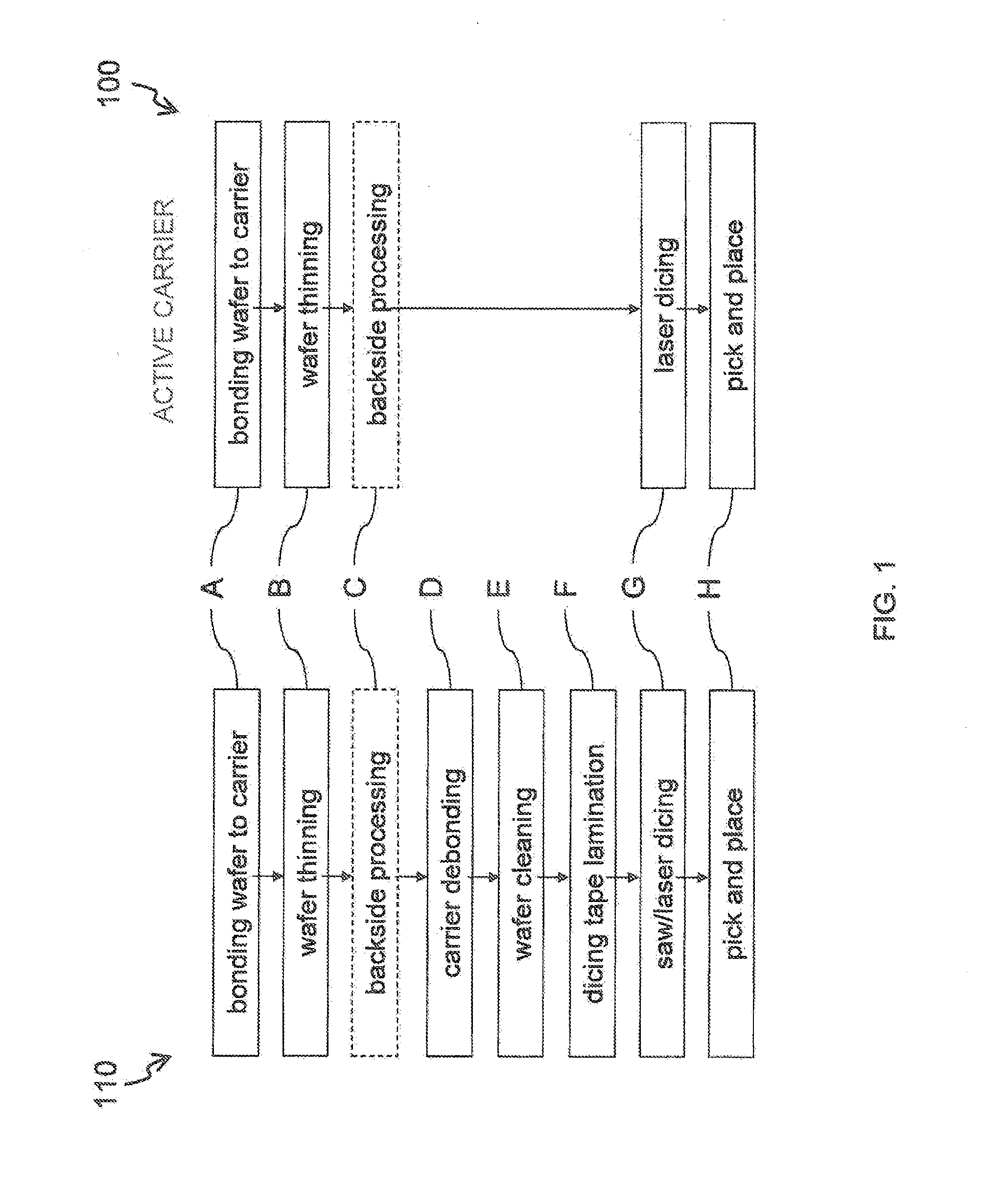
All these different steps add to the cost of ownership (CoO) of the wafer processing machine.
Currently CoO of thin wafer handling is one of the main obstacles that prevent 3D integration from reaching its full market potential.
An additional obstacle arises when removing the dies from the dicing tape (step H).
However, if the adhesion is set too high it becomes difficult to separate the obtained semiconductor dies from the adhesive tape.
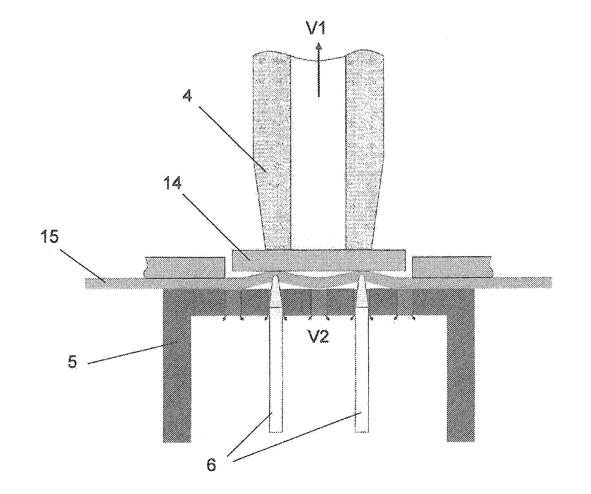
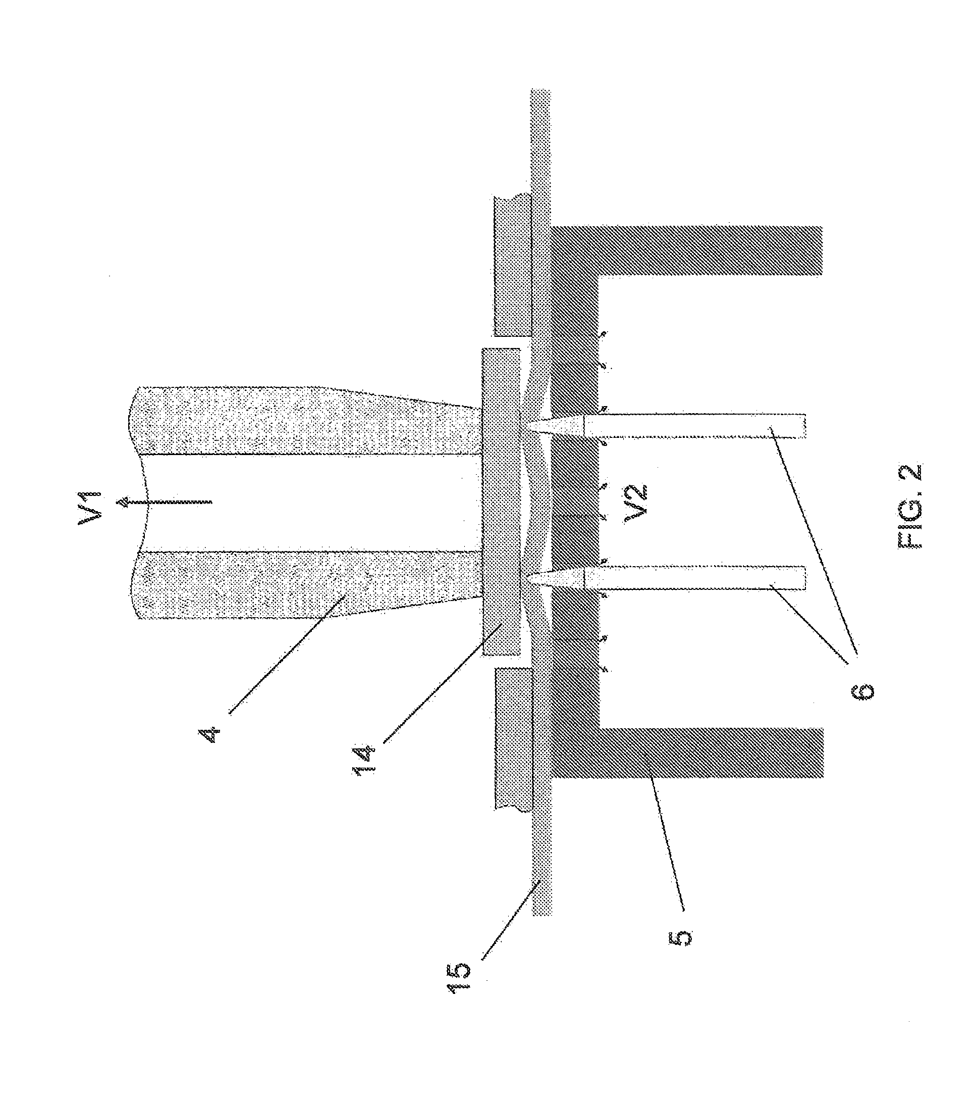
The pushing action of the needles is required as the vacuum force alone is not strong enough to overcome the adhesion and ‘squeeze-flow’ forces.
However, the pushing forces as well as the edge stresses as a result of the pushing needle only occur when the bending stiffness of the die is substantially higher than the bending stiffness of the foil.
Using slower peel speeds can help, but this will increase the cycle time and reduce productivity, resulting in increased CoO.
Further reducing chip thickness or increasing the size will result in a greater chance of the chip breaking during peeling, again increasing CoO.

Method used


Image

  • Active carrier for carrying a wafer and method for release
  • Active carrier for carrying a wafer and method for release
  • Active carrier for carrying a wafer and method for release

Examples


Embodiment Construction

[0031]Other objects, features and advantages will occur from the following description of particular embodiments and the accompanying drawings. These embodiments are described in sufficient detail to enable those skilled in the art to practice the presently disclosed systems and methods, and it is to be understood that other embodiments may be utilized and that structural and logical changes may be made without departing from the spirit and scope of the present system. In the description, identical or corresponding parts have identical or corresponding numerals. The exemplary embodiments shown should not be construed to be limitative in any manner and serve merely as illustration. The schematic symbols and shapes shown in the drawings are only used to illustrate components of the system. No particular limitation in shape, size or appearance is implied. The following detailed description is therefore not to be taken in a limiting sense, and the scope of the present system is defined ...


PUM

PropertyMeasurementUnit
thicknessaaaaaaaaaa
thicknessesaaaaaaaaaa
diameteraaaaaaaaaa

Abstract

In the field of release and pickup of ultrathin semiconductor dies, there is provided an active carrier (1) for carrying a wafer (20) and a method for using such a carrier (1). The wafer (20) comprises a particular die arrangement (P). The active carrier (1) comprises a base plate (2) and a number of energizers (7) constructed on or in this base plate (2). The energizers (7) are laid out in an arrangement corresponding to the die arrangement (P). The energizers (7) can locally energize an adhesive layer (3) in proximity to a selected die (14) from the die arrangement (P). By this local energizing of the adhesive layer (P), the selected die is loosened from the adhesive layer (3). Furthermore the active carrier (1) comprises a plurality of externally addressable contacts (12) and conduction pathways (9). The conduction pathways (9) connect the contacts (12) to the energizers (7) thereby allowing individual control over said energizers (7) by addressing said contacts (12).

Description

FIELD OF INVENTION[0001]This invention relates to an active carrier for dies.[0002]This invention further relates to a method for release and pickup of dies involving the use of an active carrierBACKGROUND OF INVENTION[0003]Typically, integrated circuits (ICs) are produced in large batches arranged on a single wafer through processes such as photolithography. This arrangement is subsequently separated into pieces called “dies”. The arrangement of the dies on the wafer (both before and after cutting) will be referred to as the die arrangement P.[0004]In the ongoing miniaturization process of IC devices, the latest developments involve the manufacture of stacks with multiple ultrathin silicon dies, also referred to as 3D stacking. Stacking is conventionally done with dies with a thickness of greater than approximately 100 micrometer.[0005]FIG. 1 shows on the left side a conventional process for transforming a (thick) wafer, with circuits formed, into a plurality of thin dies, suitable...

Claims


Application Information

Patent Timeline
Patent Type & Authority Applications(United States)
IPC IPC(8): H01L21/683H01L21/77
CPCH01L21/683H01L21/77H01L21/67132H01L2224/48091Y10T156/1911H01L2924/00014H01L21/50H01L21/67236H01L21/67721H05B3/0047
Inventor OOSTERHUIS, GERRITVAN DER ZON, CLEMENS MARIA BERNARDUSBULLEMA, JAN EITETIMMER, KLAASFISCHER, HARTMUT RUDOLFBURGHOORN, MARIA MATHEA ANTONETTA
Owner NEDERLANDSE ORG VOOR TOEGEPAST-NATUURWETENSCHAPPELIJK ONDERZOEK (TNO)
Learn More