Phase-locked loop (PLL) fail-over circuit technique and method to mitigate effects of single-event transients
a failover circuit and phase lock technology, applied in the direction of electrical equipment, pulse automatic control, etc., to achieve the effect of maintaining high quality jitter performance and minimising design complexity
- Summary
- Abstract
- Description
- Claims
- Application Information
AI Technical Summary
Benefits of technology
Problems solved by technology
Method used
Image
Examples
Embodiment Construction
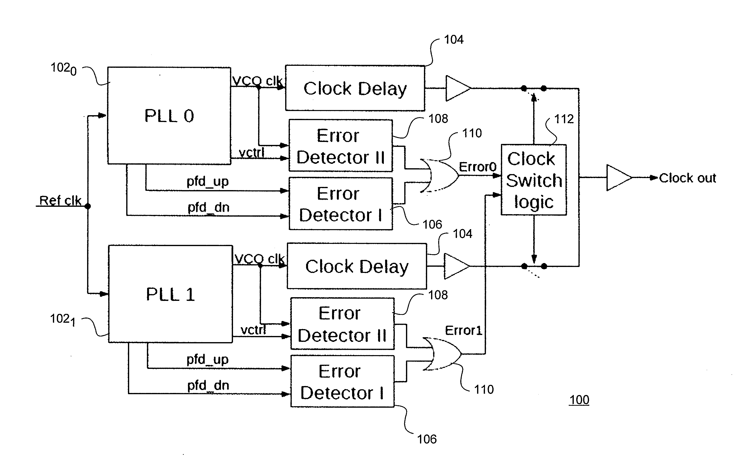
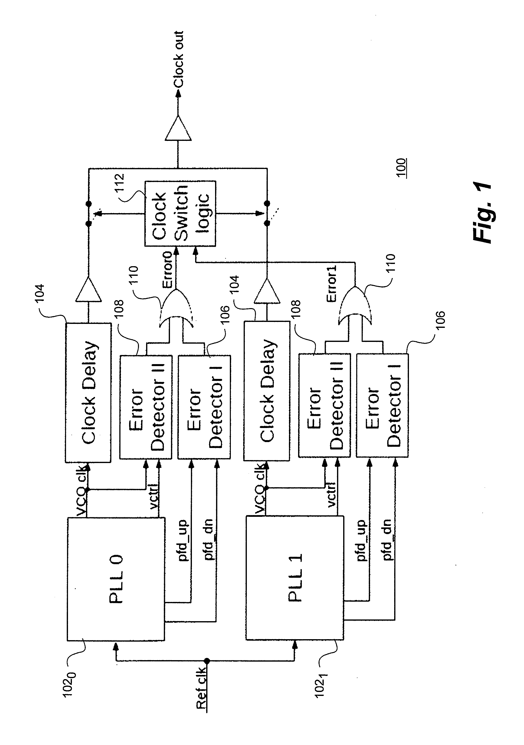
[0023]With reference now to FIG. 1, a functional block diagram of an embodiment of a PLL fail-over circuit 100 in accordance with the technique and method of the present invention is shown. The circuit 100 comprises, in pertinent part, a pair of PLL modules 1020 and 1021 each receiving a reference clock signal (Ref clk) as indicated.
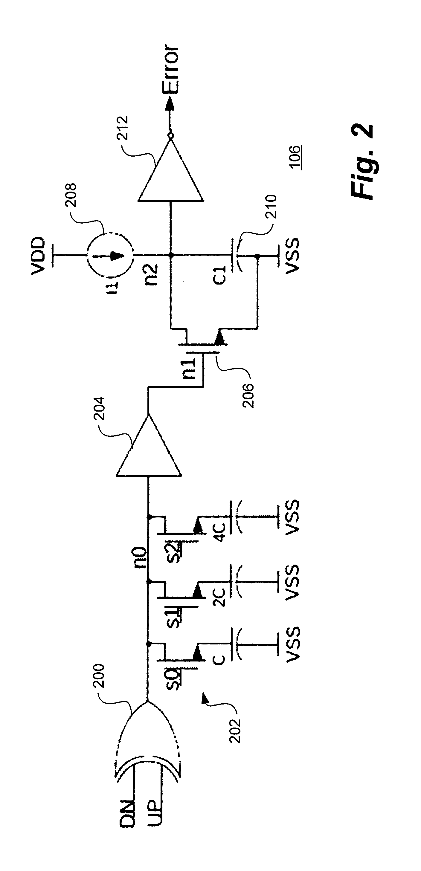
[0024]Each of the PLL modules 102 provide separate voltage controlled oscillator clock signals (VCO clk), voltage control (Vctrl) and phase-frequency detector up and down signals (pfd_up; pfd_dn) as shown. The VCO clk signals are supplied to a respective clock delay circuit 104 each of which may be conveniently provided as a number of series coupled inverters. The VCO clk signals are also furnished as one input to a respective Type II error detector circuit 108 along with the corresponding Vctrl signal. Further detail of the Type II error detector circuits 108 will be disclosed hereinafter.
[0025]The pfd_up and pfd_dn signals are provided as input to a re...
PUM
 Abstract
Description
Claims
Application Information
 - R&D
- Intellectual Property
- Life Sciences
- Materials
- Tech Scout
- Unparalleled Data Quality
- Higher Quality Content
- 60% Fewer Hallucinations
Browse by: Latest US Patents, China's latest patents, Technical Efficacy Thesaurus, Application Domain, Technology Topic, Popular Technical Reports.
© 2025 PatSnap. All rights reserved.Legal|Privacy policy|Modern Slavery Act Transparency Statement|Sitemap|About US| Contact US: help@patsnap.com


