Semiconductor device and method for producing the same
a technology of semiconductor devices and semiconductors, applied in the direction of semiconductor devices, basic electric elements, electrical equipment, etc., can solve the problems of high reverse breakdown voltage and low on-resistance of high current switching devices, and achieve the effect of reducing the concentration of electric field in the off-state in the bottom portion of the opening
- Summary
- Abstract
- Description
- Claims
- Application Information
AI Technical Summary
Benefits of technology
Problems solved by technology
Method used
Image


Examples
first embodiment
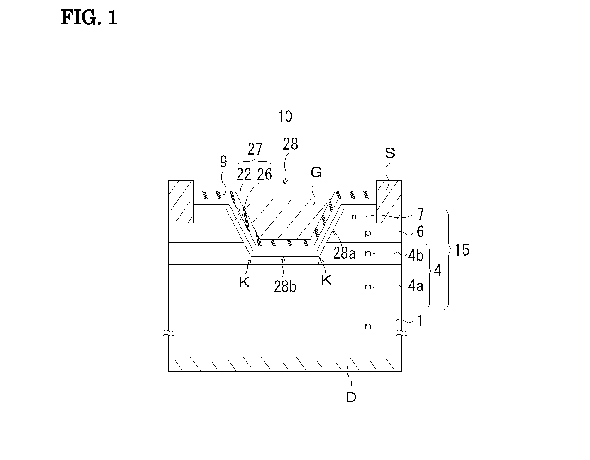
[0065]FIG. 1 is a sectional view of a vertical GaN-based FET (semiconductor device) 10 according to a first embodiment of the present invention. The vertical GaN-based FET 10 includes a conductive GaN substrate 1 and n−-type GaN drift layer 4 / p-type GaN barrier layer 6 / n+-type GaN contact layer 7 epitaxially grown on the GaN substrate 1. The n−-type GaN drift layer 4 includes a first GaN drift layer 4a located on the substrate side and a second GaN drift layer 4b that forms a bottom portion 28b of an opening. The n-type impurity concentration n2 in the second GaN drift layer 4b is lower than the n-type impurity concentration n1 in the first GaN drift layer 4a. The feature of the semiconductor device 10 of this embodiment is that the n−-type GaN drift layer 4 is divided into two layers and the n-type impurity concentration n2 in the second GaN drift layer that forms the bottom portion 28b of the opening 28 is low as described above. The condition that the n-type impurity concentratio...
second embodiment
[0090]FIG. 9 is a diagram showing a semiconductor device according to a second embodiment of the present invention. The feature of this embodiment is that a plate-shaped bottom p-type region 31 is disposed in the bottom portion 28b of the opening. The drift layer is formed of a single n−-type GaN drift layer 4. Other structures are the same as those of the semiconductor device 10 in the first embodiment (refer to FIG. 1).
[0091]The plate-shaped bottom p-type region 31 is in contact with the regrown layer 27 on the opening 28 side and forms a pn junction with the n−-type GaN drift layer 4 on the substrate 1 side. At the pn junction, a depletion layer is formed under the application of reverse bias voltage in the off-state and a voltage drop can be provided at the pn junction. Furthermore, a potential barrier formed at the pn junction also contributes to the voltage drop with certainty under the application of reverse bias voltage, which decreases the electric potential in a portion of...
examples
[0105]Regarding the semiconductor device of the first embodiment shown in FIG. 1, the reduction in the electric field concentration at the edge of the bottom portion of the opening 28 was investigated using a computer simulation. The structure of the semiconductor device 10 is as follows.[0106]4a>: thickness 5 μm, all test specimens had the same n-type impurity concentration of 1×10¹⁶ (1E16) cm−3 [0107]4b>: thickness 0.3 μm, n-type impurity concentration (A1) 1×10¹⁴ (1E14) cm−3, (A2) 1×10¹⁵ (1E15) cm−3, (A3) 1×10¹⁶ (1E16) cm−3, (B1) 5×10¹⁶ (5E16) cm−3, (B2) 1×10¹⁷ (1E17) cm−3
[0108]In the test specimens (A1) to (A3), the n-type impurity concentration in the second GaN drift layer 4b is lower than the n-type impurity concentration in the first GaN drift layer 4a. The test specimens (A1) to (A3) are treated as Invention Examples A1 to A3. In a strict sense, the test specimen (A3) having an n-type impurity concentration of 1×10¹⁶ (1E16) cm−3 cannot be treated as Invention Example. Howe...
PUM
 Abstract
Description
Claims
Application Information
 - R&D
- Intellectual Property
- Life Sciences
- Materials
- Tech Scout
- Unparalleled Data Quality
- Higher Quality Content
- 60% Fewer Hallucinations
Browse by: Latest US Patents, China's latest patents, Technical Efficacy Thesaurus, Application Domain, Technology Topic, Popular Technical Reports.
© 2025 PatSnap. All rights reserved.Legal|Privacy policy|Modern Slavery Act Transparency Statement|Sitemap|About US| Contact US: help@patsnap.com