MEMS device and method of forming the same
- Summary
- Abstract
- Description
- Claims
- Application Information
AI Technical Summary
Benefits of technology
Problems solved by technology
Method used
Image

Examples
Embodiment Construction
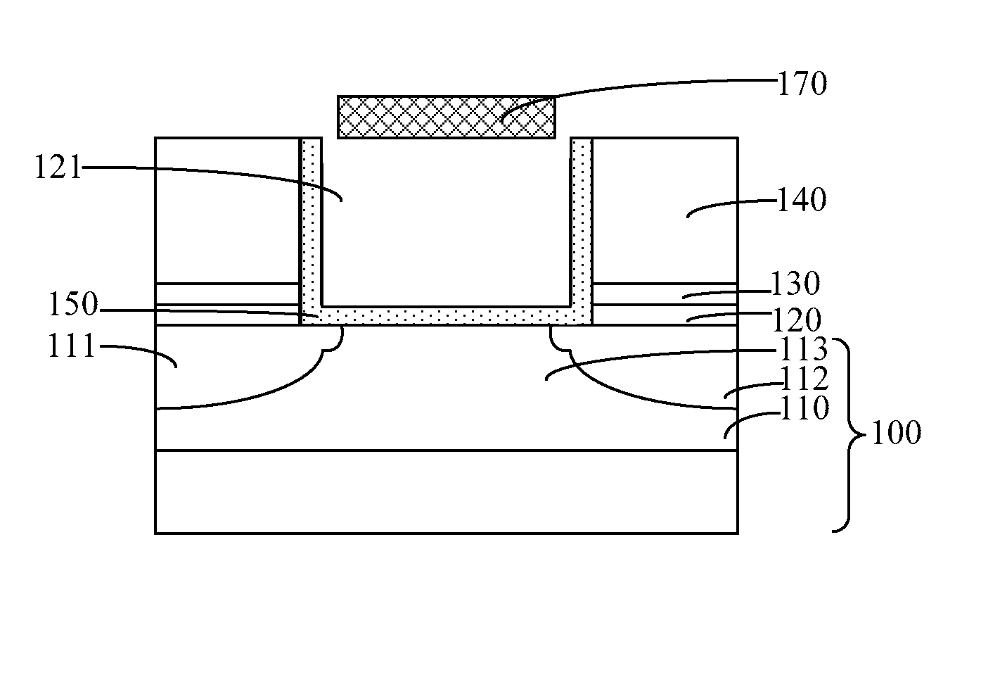
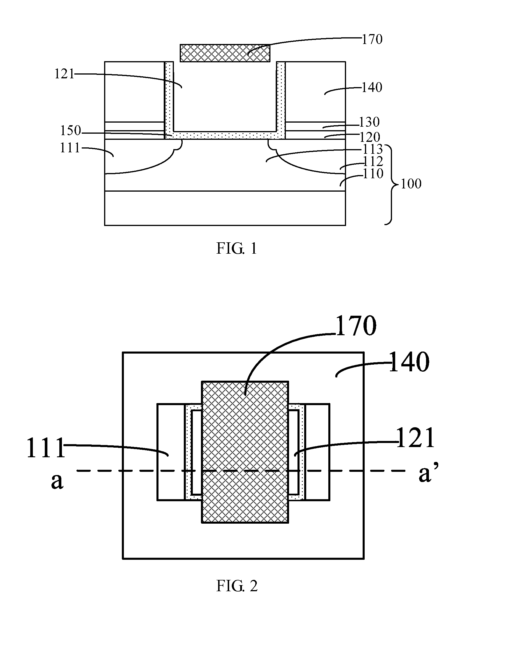
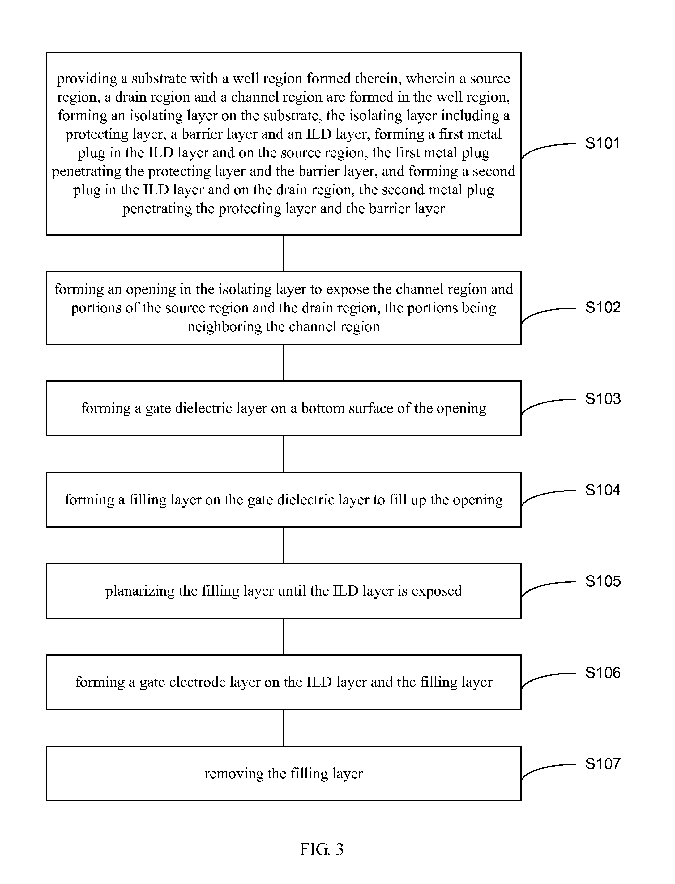
[0036]As described in the background of the present disclosure, the conventional gate structure of a transistor includes a gate dielectric layer and a gate electrode layer formed on the gate dielectric layer. Due to the material difference between the gate dielectric layer and the gate electrode layer, leakage current may occur, which affect the normal operation of the transistor.
[0037]Therefore, embodiments of the present disclosure provide a MEMS device and a method for forming the same. The MEMS device includes a gate dielectric layer and a gate electrode layer, with a gap disposed between the gate dielectric layer and the gate electrode layer. The gate electrode layer is absorbed to or floated above the gate dielectric layer by electrostatic force, thereby controlling the switch of the MEMS device. By employing the device or the method, the leakage current between the gate dielectric layer and the gate electrode layer in the semiconductor device may be avoided. Furthermore, the ...
PUM
 Abstract
Description
Claims
Application Information
 - R&D
- Intellectual Property
- Life Sciences
- Materials
- Tech Scout
- Unparalleled Data Quality
- Higher Quality Content
- 60% Fewer Hallucinations
Browse by: Latest US Patents, China's latest patents, Technical Efficacy Thesaurus, Application Domain, Technology Topic, Popular Technical Reports.
© 2025 PatSnap. All rights reserved.Legal|Privacy policy|Modern Slavery Act Transparency Statement|Sitemap|About US| Contact US: help@patsnap.com