Targeted temperature compensation in chemical vapor deposition systems

a temperature compensation and chemical vapor deposition technology, applied in the field of semiconductor fabrication technology, can solve problems such as source heat, and achieve the effect of good absorption of substrate materials

Inactive Publication Date: 2013-07-04
VEECO INSTR
View PDF0 Cites 9 Cited by
  • Summary
  • Abstract
  • Description
  • Claims
  • Application Information

AI Technical Summary

Problems solved by technology

However, the general heat source applies heat to relatively large areas.

Method used


Image

  • Targeted temperature compensation in chemical vapor deposition systems
  • Targeted temperature compensation in chemical vapor deposition systems
  • Targeted temperature compensation in chemical vapor deposition systems

Examples


Embodiment Construction

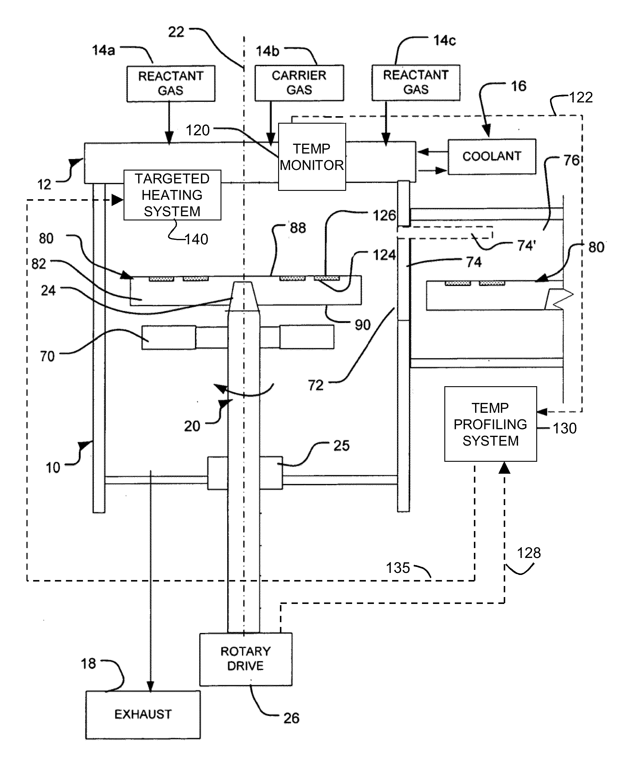
[0023]FIG. 1 illustrates a chemical vapor deposition apparatus in accordance with one embodiment of the invention. A reaction chamber 10 defines a process environment space. A gas distribution device 12 is arranged at one end of the chamber. The end having the gas distribution device 12 is referred to herein as the “top” end of the chamber 10. This end of the chamber typically, but not necessarily, is disposed at the top of the chamber in the normal gravitational frame of reference. Thus, the downward direction as used herein refers to the direction away from the gas distribution device 12; whereas the upward direction refers to the direction within the chamber, toward the gas distribution device 12, regardless of whether these directions are aligned with the gravitational upward and downward directions. Similarly, the “top” and “bottom” surfaces of elements are described herein with reference to the frame of reference of chamber 10 and gas distribution device 12.

[0024]Gas distribut...


PUM

PropertyMeasurementUnit
temperatureaaaaaaaaaa
thickaaaaaaaaaa
diameteraaaaaaaaaa

Abstract

Targeted temperature compensation for use with a chemical vapor deposition (CVD) apparatus. A localized temperature monitoring system is configured to provide localized temperature information representing surface temperatures of portions of the one or more wafers on a wafer carrier while the wafer carrier is rotating in a CVD process. A temperature profiling system is configured to generate a temperature profile that is indicative of localized cold spots on a surface of the one or more wafers. The temperature profile is based on the localized temperature information. A targeted heating system is configured to selectively apply localized heat to the localized cold spots dynamically based on the temperature profile such that a thermal distribution of the surface of the one or more wafers is made more uniform while a CVD process is carried out on the CVD apparatus.

Description

FIELD OF THE INVENTION[0001]The invention relates generally to semiconductor fabrication technology and, more particularly, to chemical vapor deposition (CVD) processing and associated apparatus for correcting temperature non-uniformities on semiconductor wafer surfaces.BACKGROUND OF THE INVENTION[0002]In the fabrication of light-emitting diodes (LEDs) and other high-performance devices such as laser diodes, optical detectors, and field effect transistors, a chemical vapor deposition (CVD) process is typically used to grow a thin film stack structure using materials such as gallium nitride over a sapphire or silicon substrate. A CVD tool includes a process chamber, which is a sealed environment that allows infused gases to be deposited upon the substrate (typically in the form of wafers) to grow the thin film layers. A number of process parameters are controlled, such as temperature, pressure and gas flow rate, to achieve a desired crystal growth. Different layers are grown using va...

Claims


Application Information

Patent Timeline
Patent Type & Authority Applications(United States)
IPC IPC(8): C30B25/10C30B25/16
CPCC30B25/10C30B25/16
Inventor SHAMOUN, BASSAM
Owner VEECO INSTR
Why Eureka
Try Eureka