Clock and data recovery circuit
a clock and data recovery technology, applied in the direction of electrical equipment, pulse automatic control, etc., can solve the problem of increasing the bit error rate (ber)
- Summary
- Abstract
- Description
- Claims
- Application Information
AI Technical Summary
Benefits of technology
Problems solved by technology
Method used
Image
Examples
Embodiment Construction
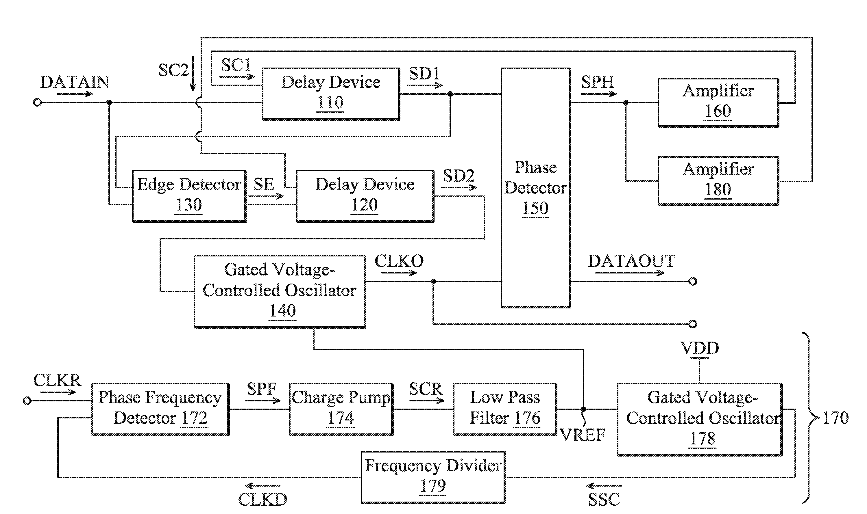
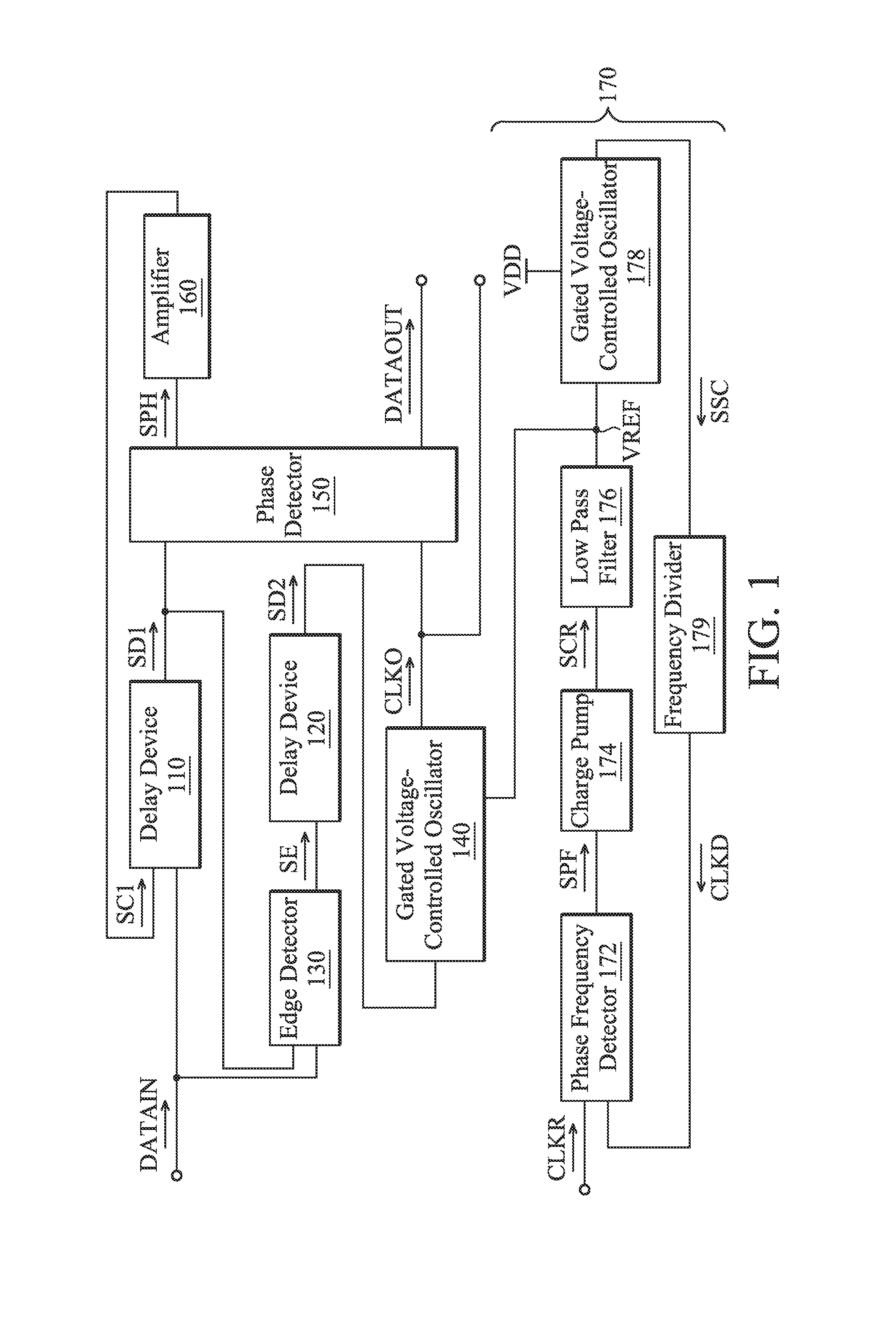
[0015]FIG. 1 is a diagram for illustrating a clock and data recovery (CDR) circuit 100 according to an embodiment of the invention. As shown in FIG. 1, the CDR circuit 100 comprises: delay devices 110 and 120, an edge detector 130, a gated voltage-controlled oscillator (GVCO) 140, a phase detector 150, an amplifier 160, and a phase locked loop (PLL) circuit 170.
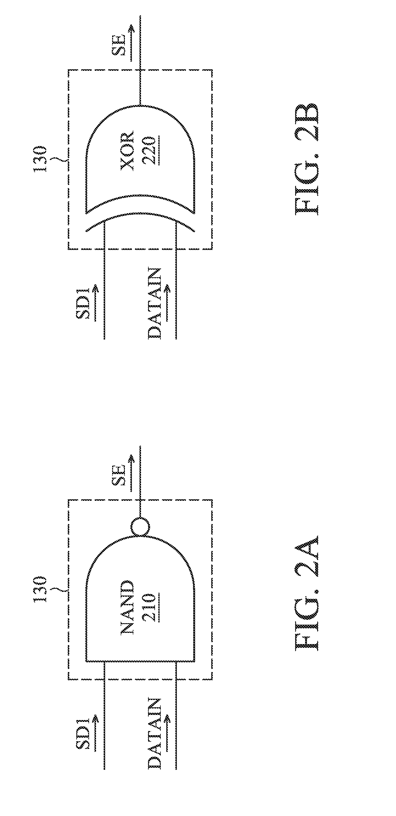
[0016]The PLL circuit 170 provides a reference voltage VREF so as to control the GVCO 140. The delay device 110 is configured to delay an input data DATAIN according to a control signal SC1 so as to generate a delay signal SD1, which is utilized for adjusting a delay time of the delay device 110. The edge detector 130 is configured to generate an edge signal SE according to the delay signal SD1 and the input data DATAIN, and more particularly, the edge detector 130 is configured to detect rising edges and / or falling edges of the delay signal SD1 and the input data DATAIN so as to generate the edge signal SE. The delay device ...
PUM
 Abstract
Description
Claims
Application Information
 - R&D
- Intellectual Property
- Life Sciences
- Materials
- Tech Scout
- Unparalleled Data Quality
- Higher Quality Content
- 60% Fewer Hallucinations
Browse by: Latest US Patents, China's latest patents, Technical Efficacy Thesaurus, Application Domain, Technology Topic, Popular Technical Reports.
© 2025 PatSnap. All rights reserved.Legal|Privacy policy|Modern Slavery Act Transparency Statement|Sitemap|About US| Contact US: help@patsnap.com


