
System-in-package module and method of fabricating the same

a technology of system-in-package module and packaging module, which is applied in the direction of semiconductor devices, electrical equipment, semiconductor/solid-state device details, etc., can solve the problems of increasing design complexity and fabrication cost, and the shielding lid cannot be mounted to the package module, so as to reduce design complexity and fabrication cost, and increase design flexibility. , the effect of less spa

Inactive Publication Date: 2013-05-30
ASKEY TECH JIANGSU +1
View PDF0 Cites 2 Cited by
  • Summary
  • Abstract
  • Description
  • Claims
  • Application Information

AI Technical Summary

Benefits of technology

The present invention provides a SiP module and method of fabrication that protects against electromagnetic radiation interference, while also reducing space consumption, design complexity, fabrication cost and increasing design flexibility. The shielding layer formed on the ground vias helps to ground electromagnetic radiations, replacing the prior art's shielding lid. Overall, the SiP module is better protected, takes up less space, and has greater design flexibility.

Problems solved by technology

However, the shielding lid occupies too much the space in the package module, leaving less space for patterning of circuits.
But after the molding process, the shielding lid cannot be mounted to the package module.
Therefore, the package module cannot be protected against electromagnetic radiation interferences.
However, such a system requires additional components, thereby increasing the design complexity and the fabrication cost.
In addition, since the recess corresponds in position to the package module, the positions of the recess and the package module are limited by each other, thus reducing the design flexibility.

Method used


Image

  • System-in-package module and method of fabricating the same
  • System-in-package module and method of fabricating the same
  • System-in-package module and method of fabricating the same

Examples


Embodiment Construction

[0018]The following illustrative embodiments are provided to illustrate the disclosure of the present invention, these and other advantages and effects can be apparent to those in the art after reading this specification.

[0019]It should be noted that all the drawings are shown for illustrative purposes only and not intended to limit the present invention.

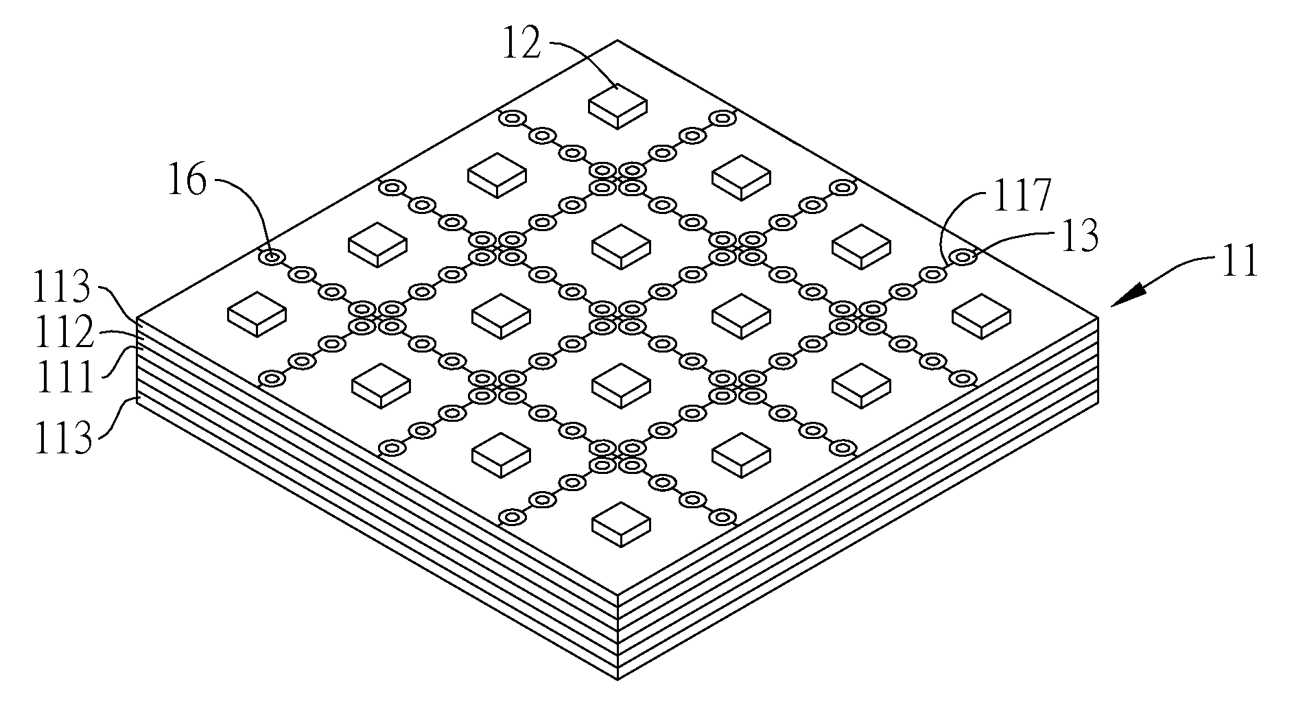
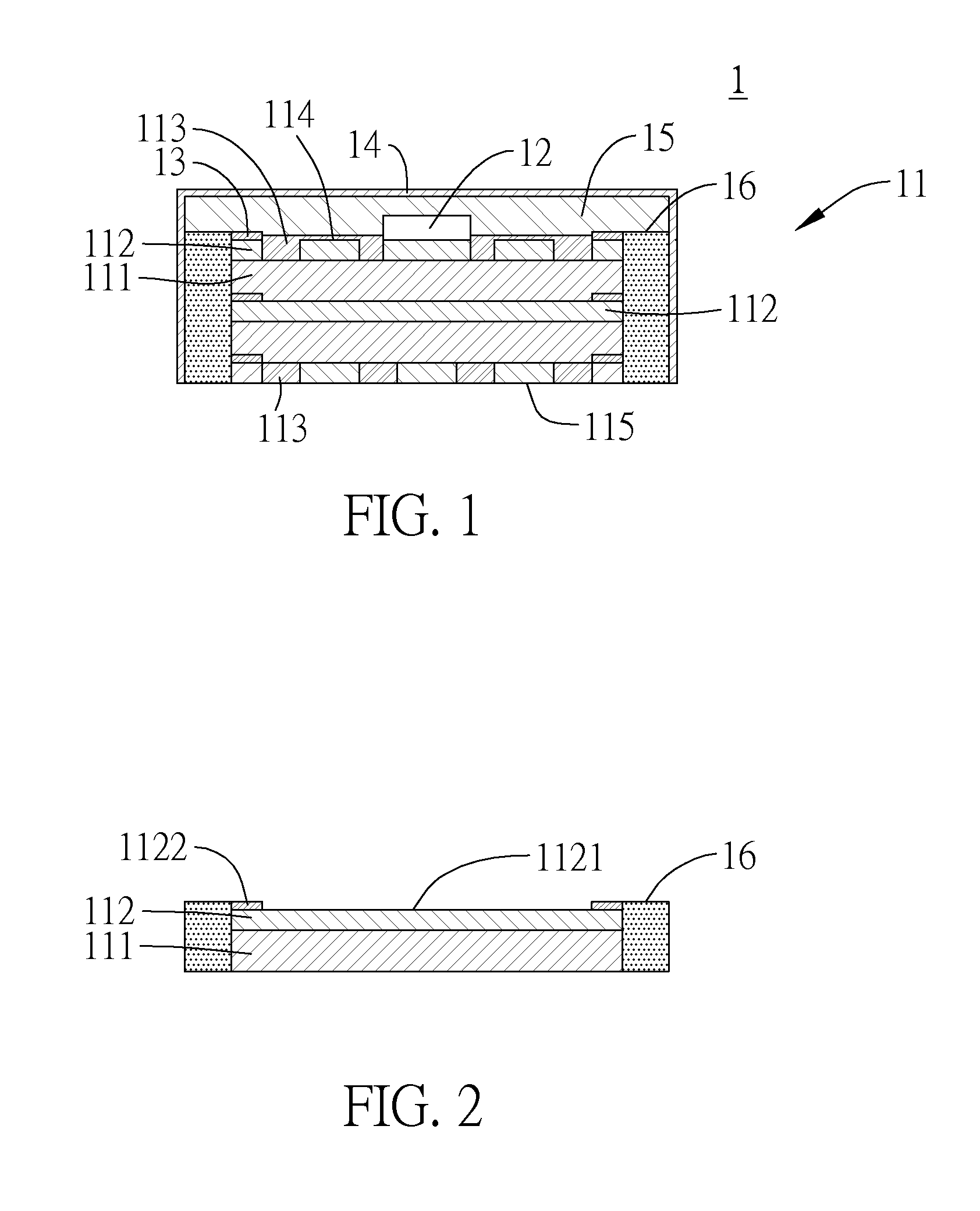
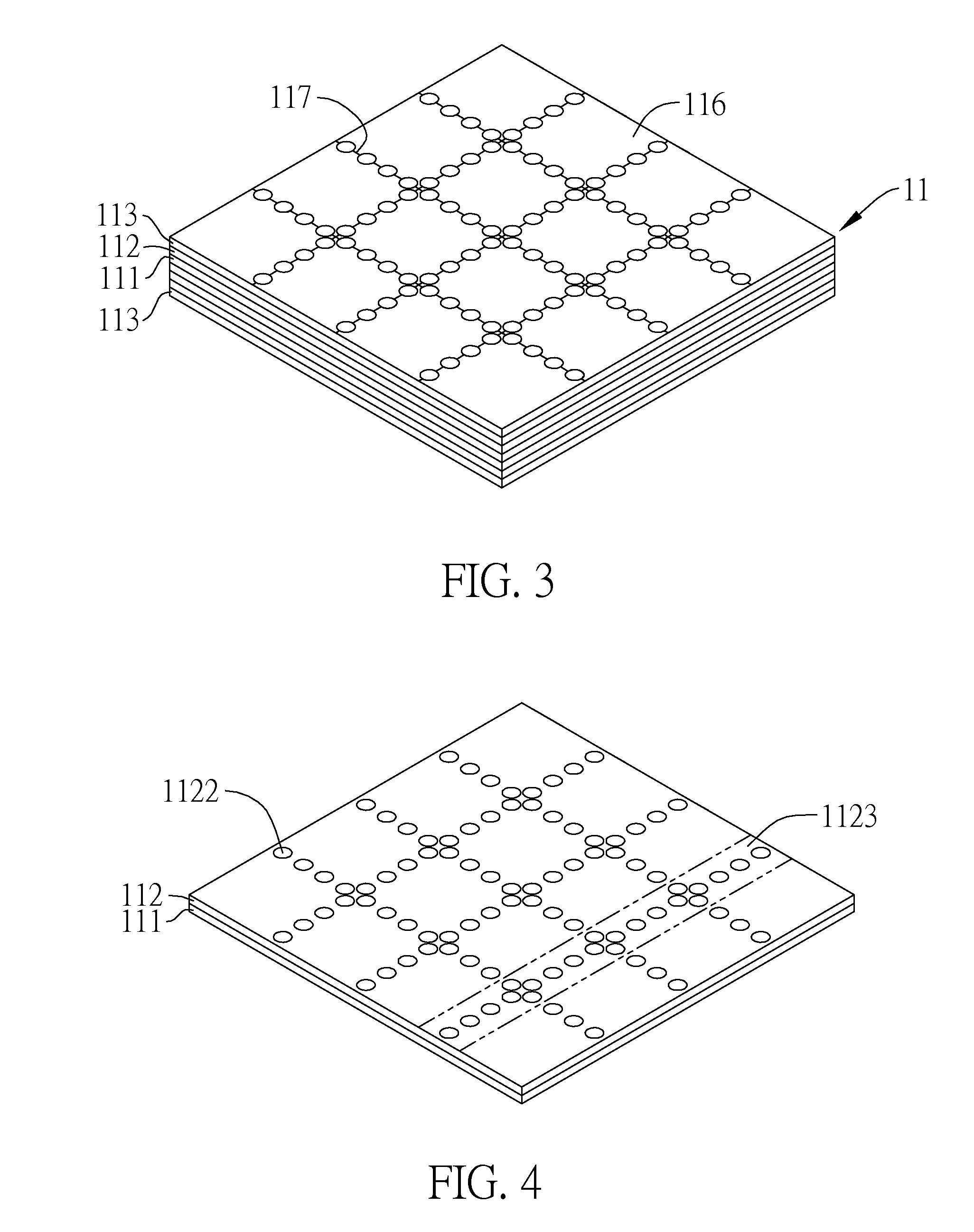
[0020]FIG. 1 is a schematic cross-sectional view of a SiP module 1 according to the present invention. The SiP module 1 has a substrate 11 having a plurality of ground vias 16 penetrating therethrough, an electronic component 12 and a plurality of ground pads 13 disposed on the substrate 11, an encapsulant 15 formed on the substrate 11 for encapsulating the electronic component 12, and a shielding layer 14 formed to cover the encapsulant 15 and the ground vias 16. It should be noted that the SiP module 1 can be applied to various kinds of package modules. In an embodiment, the electronic component 12 is, for example, a semiconductor...


PUM


Abstract

A method of fabricating a system-in-package (SiP) module is provided, which includes: providing a substrate having a plurality of scribe lines formed thereon, forming ground pads and ground vias along the scribe lines, disposing at least one electronic component on the substrate, forming on the substrate an encapsulant for encapsulating the electronic component, cutting the substrate along the scribe lines so as to expose the ground vias, and forming a shielding layer on the encapsulant and the ground vias to thereby obtain a plurality of SiP modules. Therefore, electromagnetic radiation interferences are avoided and the design complexity and fabrication cost are reduced.

Description

BACKGROUND OF THE INVENTION[0001]1. Field of the Invention[0002]The present invention relates to package module technologies, and, more particularly, to a system-in-package (SiP) module and a method of fabricating the same.[0003]2. Description of Related Art[0004]Electromagnetic compatibility (EMC) is an important research subject in the electromagnetic field, and how to prevent electromagnetic interferences is an important issue in the fabrication of package modules.[0005]Conventionally, after a package module is produced, a shielding lid is mounted to an outer periphery of the package module for protecting the package module against electromagnetic radiation interferences. However, the shielding lid occupies too much the space in the package module, leaving less space for patterning of circuits.[0006]In fabricating a system-in-package (SiP) module, a molding process is employed by certain manufacturers so as for the package module to have the same appearance as an integrated circu...

Claims


Application Information

Patent Timeline
Patent Type & Authority Applications(United States)
IPC IPC(8): H01L23/552H01L21/56
CPCH01L23/552H01L24/97H01L23/49805H01L21/561H01L2924/01029H01L2924/12042H01L2924/00
Inventor CHEN, CHI-SHENGHSIEH, CHING-FENG
Owner ASKEY TECH JIANGSU
Learn More