Electrostatic discharge (ESD) device and semiconductor structure
a technology of electrostatic discharge and semiconductor structure, which is applied in the direction of semiconductor devices, semiconductor/solid-state device details, electrical apparatus, etc., can solve the problem of inability to detect the ab layer, and achieve the effect of increasing the device dimension and high esd robustness
- Summary
- Abstract
- Description
- Claims
- Application Information
AI Technical Summary
Benefits of technology
Problems solved by technology
Method used
Image

Examples
first embodiment
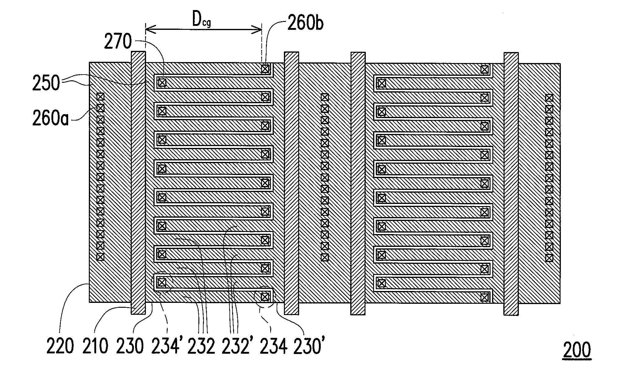
[0019]FIG. 2 illustrates a layout of a series of ESD devices and the derivative semiconductor structure according to this invention.
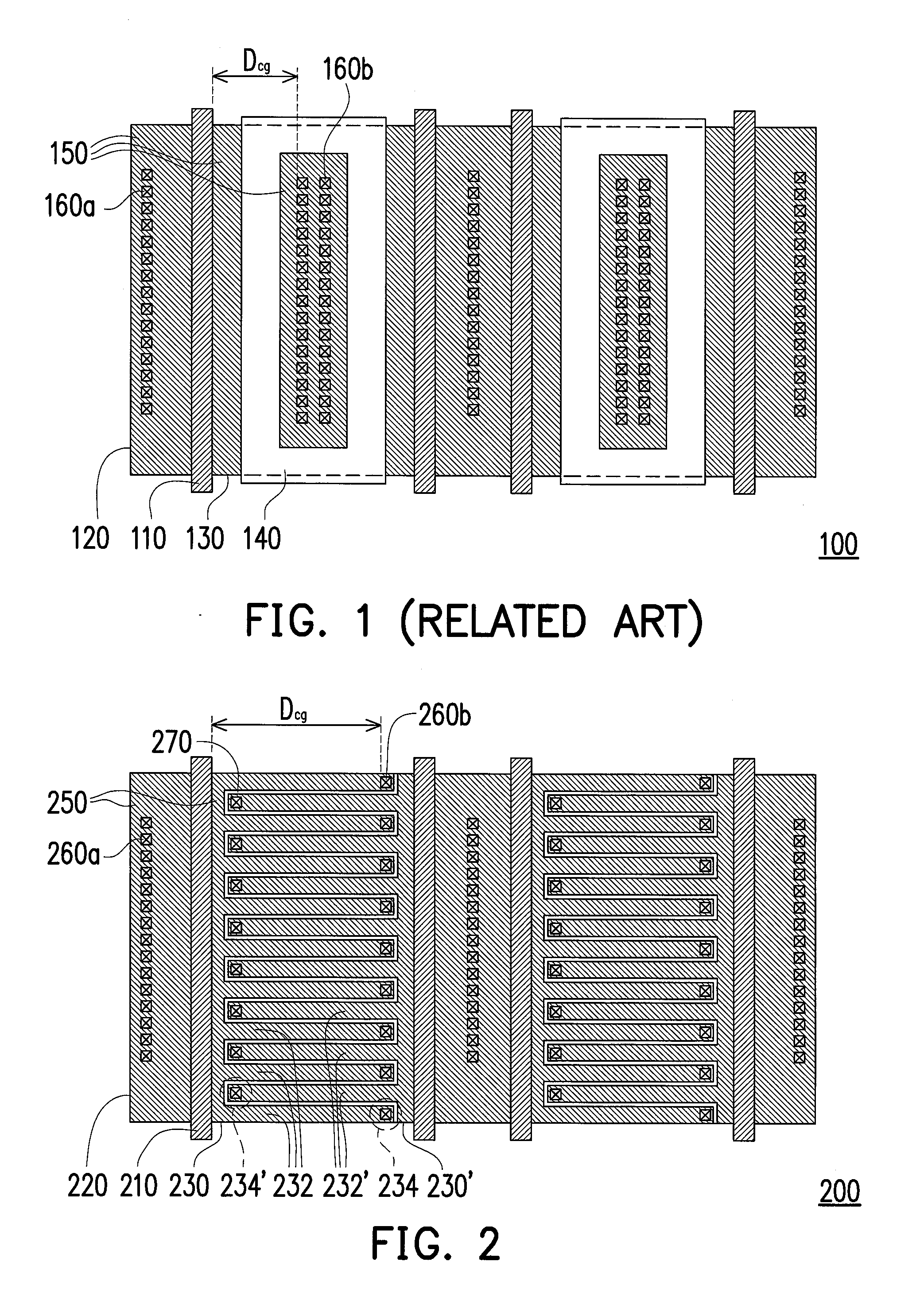
[0020]Referring to FIG. 1, each of the ESD devices includes a gate line 210 disposed on a semiconductor substrate 200, a source region 220 in the substrate 200 at a first side of the gate line 210, a comb-shaped drain region 230 disposed in the substrate 200 at a second side of the gate line 210 and having a plurality of comb-teeth parts 232, a salicide layer 250 on the source region 220 and the drain region 200, a plurality of contact plugs 260a on the salicide layer 250 on the source region 220, and a plurality of contact plugs 260b on the salicide layer 250 on the drain region 230. Each comb-teeth part 232 of the comb-shaped drain region 230 has thereon, at the tip portion 234 thereof, a contact plug 260b. An ESD device may share a source region 220 with an adjacent ESD device, as shown in the figure.
[0021]The semiconductor substrate 200 may be a lig...
second embodiment
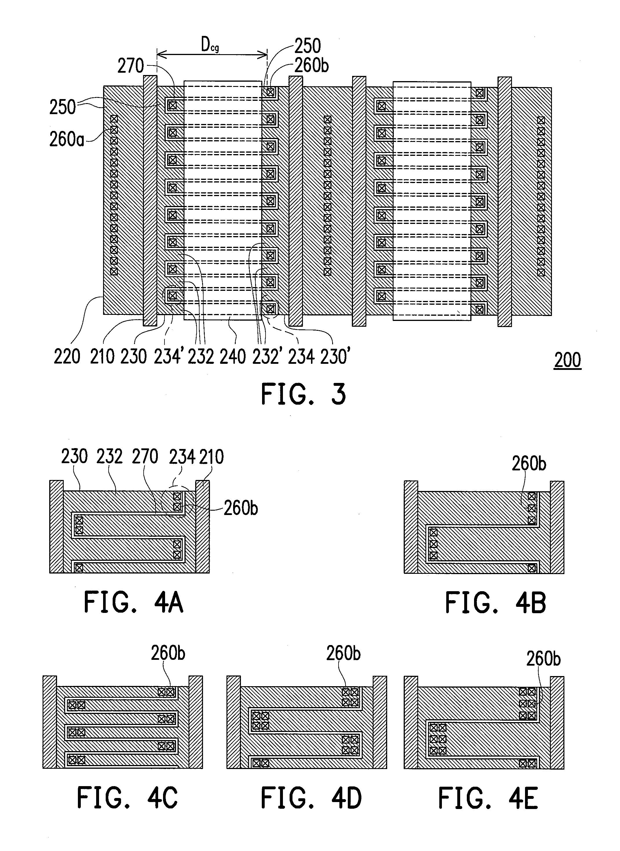
[0023]Besides, when the IC process includes formation of salicide block (SAB), a SAB layer may be formed before the salicide layer 250 is formed. Such an embodiment is shown in FIG. 3, which illustrates a layout of a series of ESD devices and the derivative semiconductor structure according to this invention.
[0024]The major difference of the ESD device or the semiconductor structure of the second embodiment from that of the first embodiment include that a SAB layer 240 is further disposed covering a portion of each comb-teeth part 232 / 232′ of each drain region 230 / 230′, wherein the salicide layer 250 is not disposed on the portions of the comb-teeth parts 232 / 232′ covered by the SAB layer 240.
[0025]In an embodiment, the SAB layer 240 covers all area of each comb-teeth part 232 / 232′ except its tip portion 234 / 234′ for forming a contact plug 260b and the portion thereof beside the tip portions 234′ / 234 of the neighboring comb-teeth parts 232′ / 232, so as to provide a maximal salicide-f...
PUM
 Abstract
Description
Claims
Application Information
 - R&D
- Intellectual Property
- Life Sciences
- Materials
- Tech Scout
- Unparalleled Data Quality
- Higher Quality Content
- 60% Fewer Hallucinations
Browse by: Latest US Patents, China's latest patents, Technical Efficacy Thesaurus, Application Domain, Technology Topic, Popular Technical Reports.
© 2025 PatSnap. All rights reserved.Legal|Privacy policy|Modern Slavery Act Transparency Statement|Sitemap|About US| Contact US: help@patsnap.com