Light-Emitting Module and Light-Emitting Device
a light-emitting module and light-emitting device technology, which is applied in the direction of organic semiconductor devices, semiconductor lamp usage, thermoelectric devices, etc., can solve the problems of uneven brightness of the surface from which light emission is extracted, difficulty in extracting uniform planar light emission from the light-emitting module, and failure of luminance distribution, so as to reduce the voltage drop occurring and reduce the effect of second electrod
- Summary
- Abstract
- Description
- Claims
- Application Information
AI Technical Summary
Benefits of technology
Problems solved by technology
Method used
Image

Examples
embodiment 1
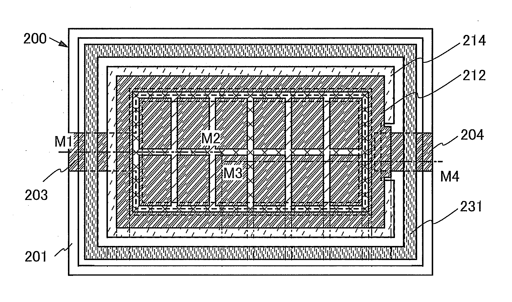
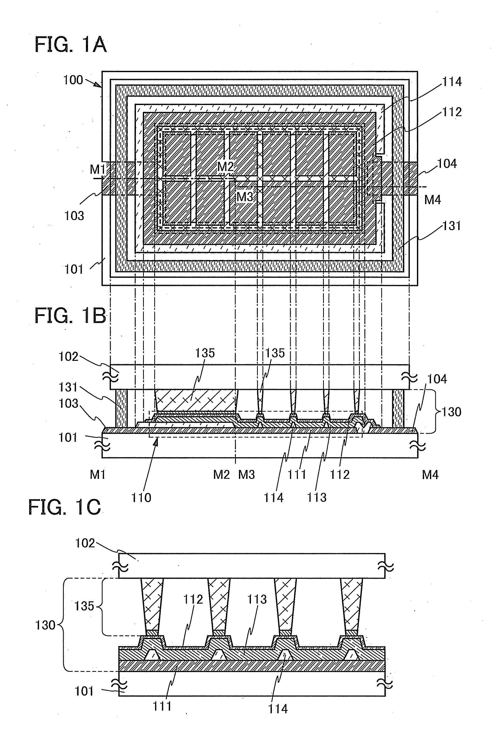
[0042]In this embodiment, a structure of a light-emitting module according to one embodiment of the present invention is described. Specifically, a light-emitting module including a first substrate, a light-emitting element, formed on one surface side of the first substrate, a second substrate provided on the one surface side of the first substrate, a conductive spacer maintaining the gap between the first substrate and the second substrate, and a space in which the light-emitting element is sealed between the first substrate and the second substrate is described. Note that a first electrode and a partition having an opening over the first electrode are provided over the first substrate. The light-emitting element includes, in a position overlapping with the opening of the partition, the first electrode, a second electrode, and a layer containing a light-emitting organic compound between the first electrode and the second electrode. The second electrode is a metal thin film formed b...
modification example 1
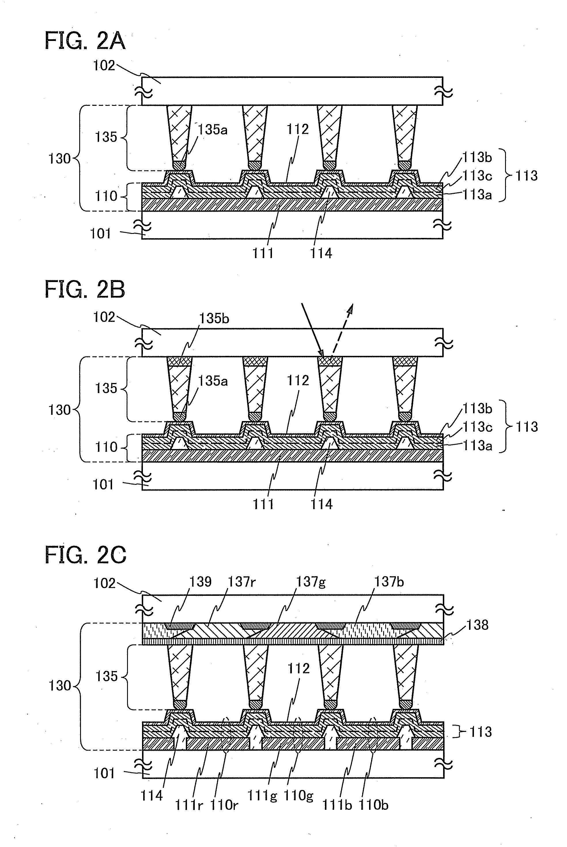
[0092]A modification example 1 of the light-emitting module of this embodiment is described with reference to FIG. 2A. In a light-emitting module shown as an example in the modification example 1, the light-emitting element 110 includes a first layer 113a containing a light-emitting organic compound, a second layer 113b containing a light-emitting organic compound, and an intermediate layer 113c. Note that the intermediate layer 113c is provided between the first layer 113a containing a light-emitting organic compound and the second layer 113b containing a light-emitting organic compound.
[0093]Further, the conductive spacer 135 has an edge 135a in which a corner portion is chamfered to have a curved surface, and the edge 135a is in contact with the second electrode 112 of the light-emitting element 110 over the partition 114.
[0094]The conductive spacer 135 is provided such that the layers formed over the partition 114 are interposed between an edge of the conductive spacer 135 and t...
modification example 2
[0100]A modification example 2 of the light-emitting module of this embodiment is described with reference to FIG. 2B. In a light-emitting module shown as an example in the modification example 2, the conductive spacer 135 includes a layer 135b with a low reflectance on the second substrate 102 side.
[0101]The layer 135b with a low reflectance is formed using a material that is unlikely to reflect outside light; for example, a colored conductive layer or a colored insulating layer can be used.
[0102]Examples of the colored conductive layer include a metal layer, a metal nitride layer, and a resin layer in which a filler is dispersed; specifically, it is possible to use gold, copper, titanium nitride, a resin in which carbon black is dispersed, or the like. Further, examples of the colored insulating layer include an insulating inorganic material layer and a resin layer in which a pigment is dispersed.
[0103]The layer 135b with a low reflectance absorbs part of outside light that enters...
PUM
 Abstract
Description
Claims
Application Information
 - R&D
- Intellectual Property
- Life Sciences
- Materials
- Tech Scout
- Unparalleled Data Quality
- Higher Quality Content
- 60% Fewer Hallucinations
Browse by: Latest US Patents, China's latest patents, Technical Efficacy Thesaurus, Application Domain, Technology Topic, Popular Technical Reports.
© 2025 PatSnap. All rights reserved.Legal|Privacy policy|Modern Slavery Act Transparency Statement|Sitemap|About US| Contact US: help@patsnap.com