


Quick Research
Generate reliable direction feasibility study reports for your R&D in just a few steps.

Technical Q&A
Discover and master advanced knowledge NOW. Basics, ideas, possibilities, all at once.

Find Solutions
As an expert in R&D theories, this can generate solutions to your technical problems instantly.

Evaluate Feasibility
Analyze your overall solution with one click, know your potential R&D risks in advance.

Monitor Landscape
Get weekly tech updates, stay abreast of the latest tech innovations and key insights.
Solid-state imaging device and imaging system
- Summary
- Abstract
- Description
- Claims
- Application Information
AI Technical Summary
Benefits of technology
Problems solved by technology
Method used
Image

Examples
Embodiment Construction
[0032]Various exemplary embodiments, features, and aspects of the invention will be described in detail below with reference to the drawings.
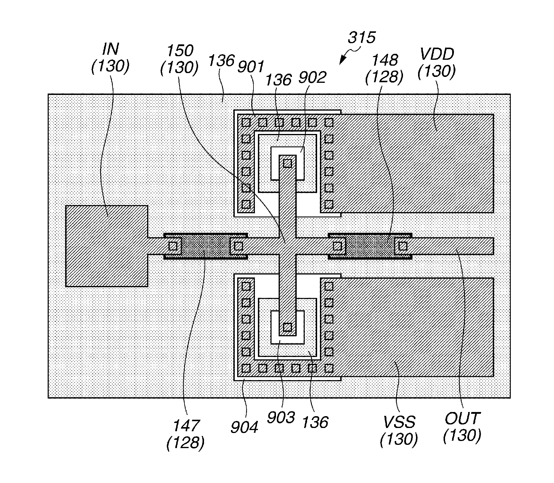
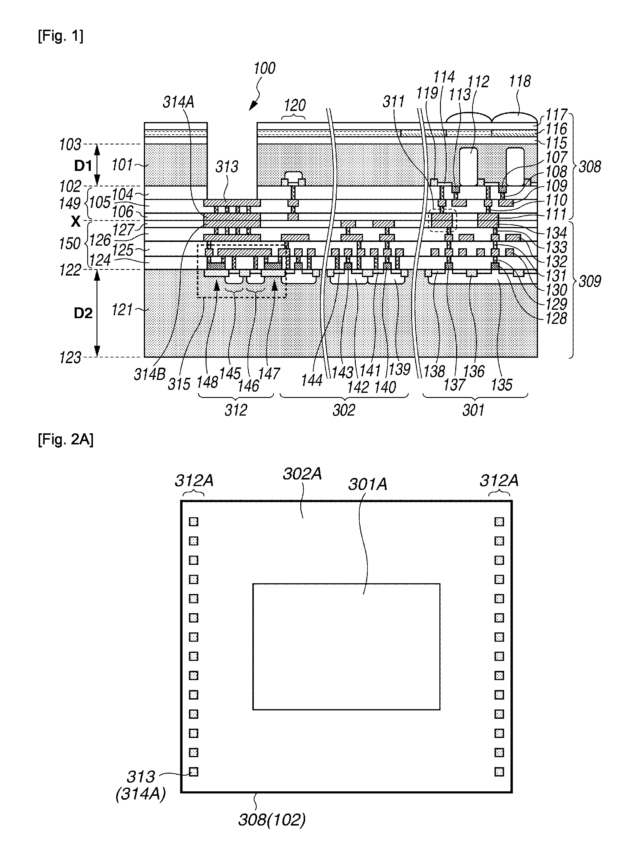
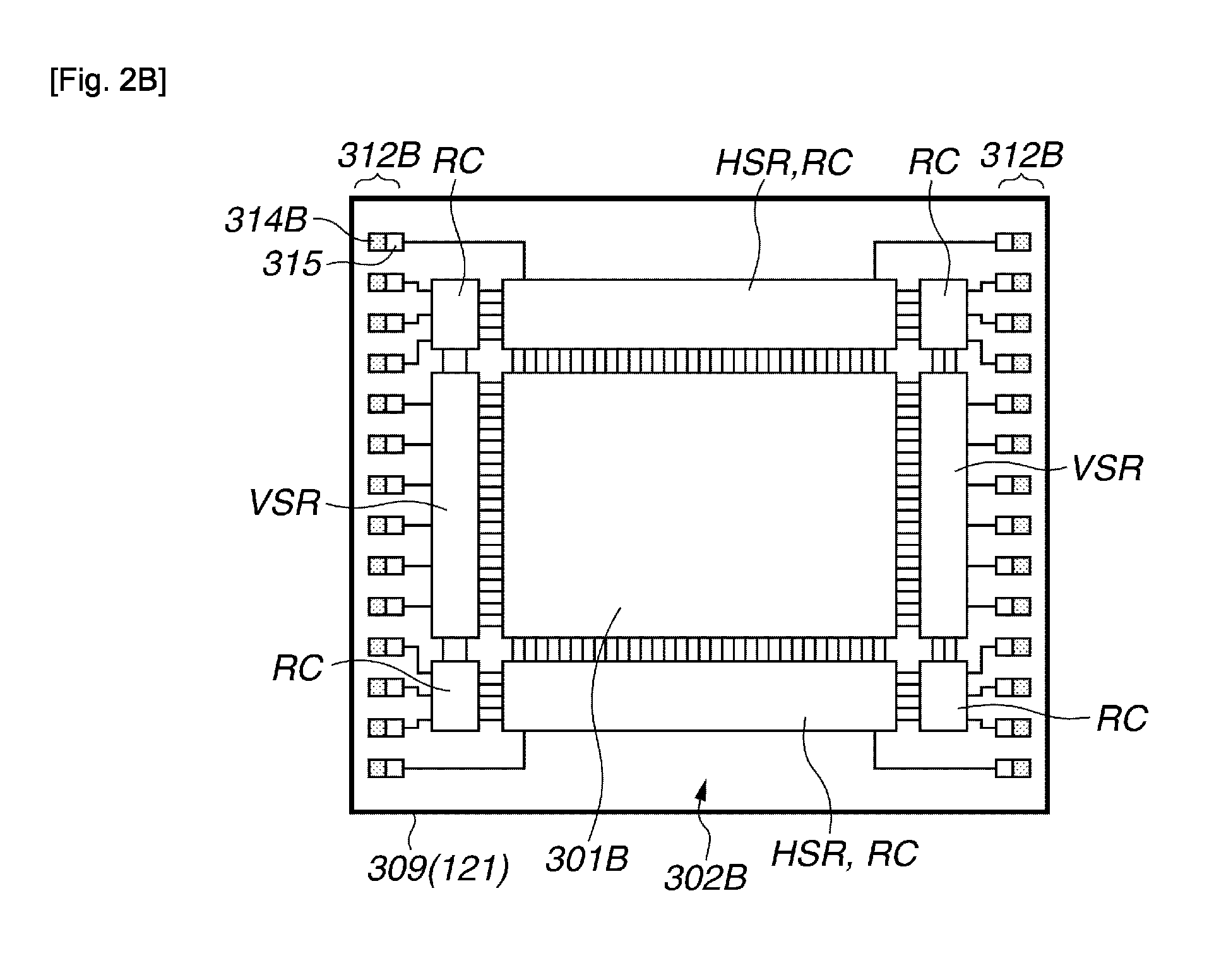
[0033]A solid-state imaging device according to the present invention comprises a first semiconductor substrate including a photoelectric conversion element, and a second semiconductor substrate including at least a part of a peripheral circuit. The peripheral circuit is for generating a signal based on the charge of the photoelectric conversion element and is arranged in a main face thereof. A main face of the first semiconductor substrate and the main face of the second semiconductor substrate are opposed to each other with sandwiching a wiring structure therebetween. The solid-state imaging device comprises a pad to be connected to an external terminal, and a protection circuit electrically connected to the pad and to the peripheral circuit. The protection circuit is arranged in the main face of the second semiconductor substrate. By thus ar...
PUM
 Abstract
Description
Claims
Application Information
 - R&D Engineer
- R&D Manager
- IP Professional
- Industry Leading Data Capabilities
- Powerful AI technology
- Patent DNA Extraction
Browse by: Latest US Patents, China's latest patents, Technical Efficacy Thesaurus, Application Domain, Technology Topic, Popular Technical Reports.
© 2024 PatSnap. All rights reserved.Legal|Privacy policy|Modern Slavery Act Transparency Statement|Sitemap|About US| Contact US: help@patsnap.com