Light source device
a light source and optical technology, applied in the field of optical devices, can solve the problems of lgp color beams that may interfere with one another, deflection of light paths, and chrominance of the subsequently displayed images of the lcd
- Summary
- Abstract
- Description
- Claims
- Application Information
AI Technical Summary
Benefits of technology
Problems solved by technology
Method used
Image
Examples
first embodiment
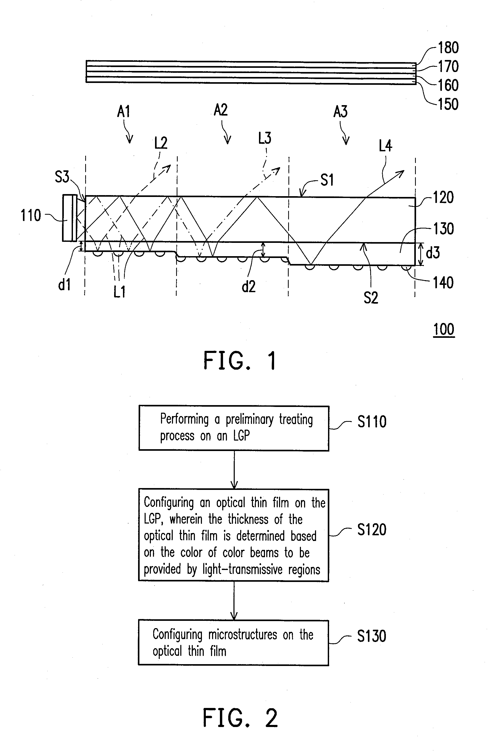
[0027]FIG. 1 is a schematic view illustrating a light source device according to a first embodiment of the invention. With reference to FIG. 1, the light source device 100 of this embodiment includes a light-emitting element 110, a light guide plate (LGP) 120, an optical thin film 130, and a plurality of microstructures 140. The light-emitting element 110 is capable of providing illumination beams L1. In this embodiment, the light-emitting element 110 is a light-emitting diode (LED), for instance, and the illumination beams L1 are white light, for instance. Here, the white light is composed of a plurality of different color beams.
[0028]As shown in FIG. 1, the light-emitting element 110 is located beside the LGP 120, and the LGP 120 is divided into a plurality of light-transmissive regions A1˜A3 (three light-transmissive regions A1˜A3 are shown in the drawings for example, which should not be construed as a limitation to the invention). The LGP 120 has a surface S1, a surface S2, and...
second embodiment
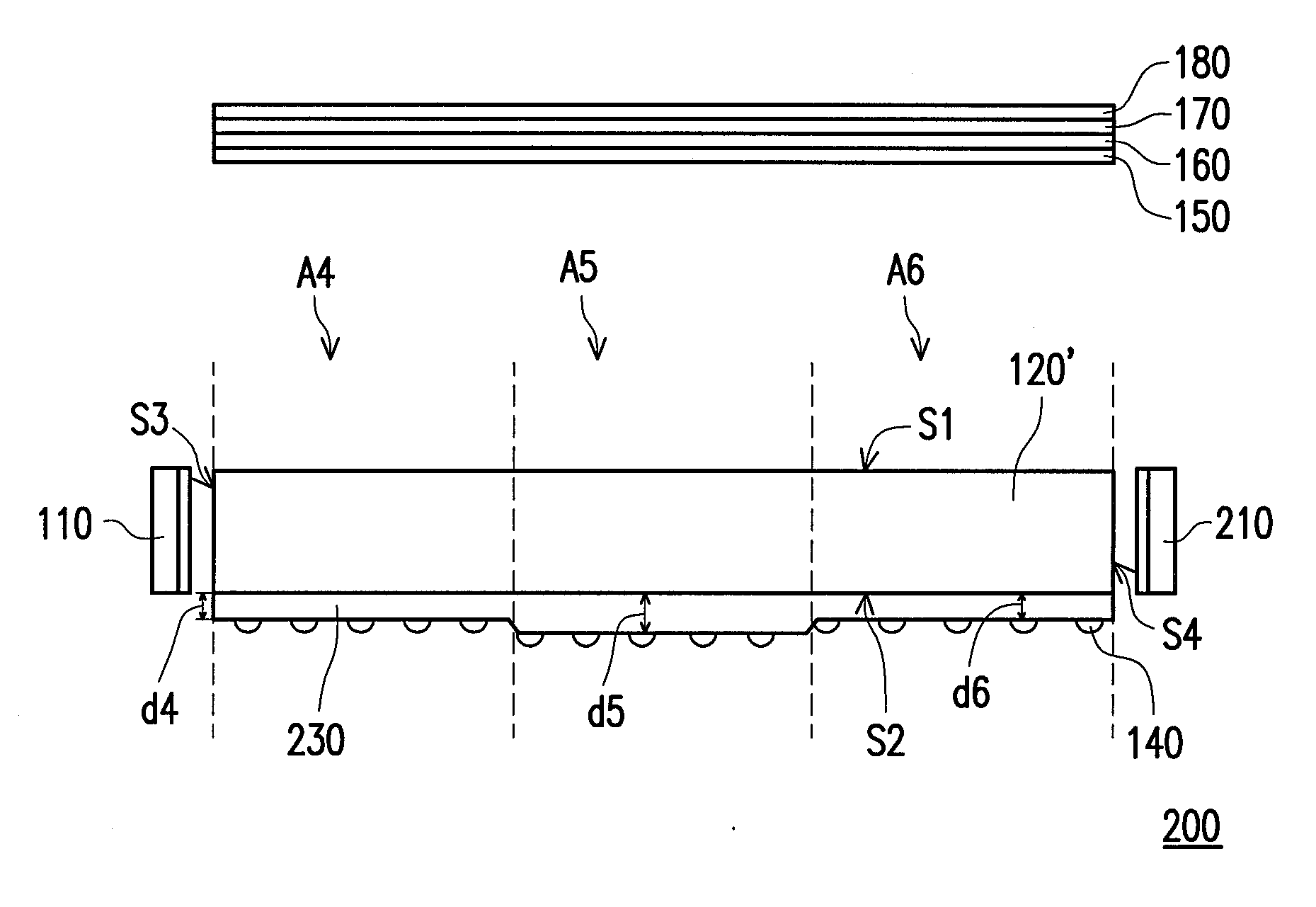
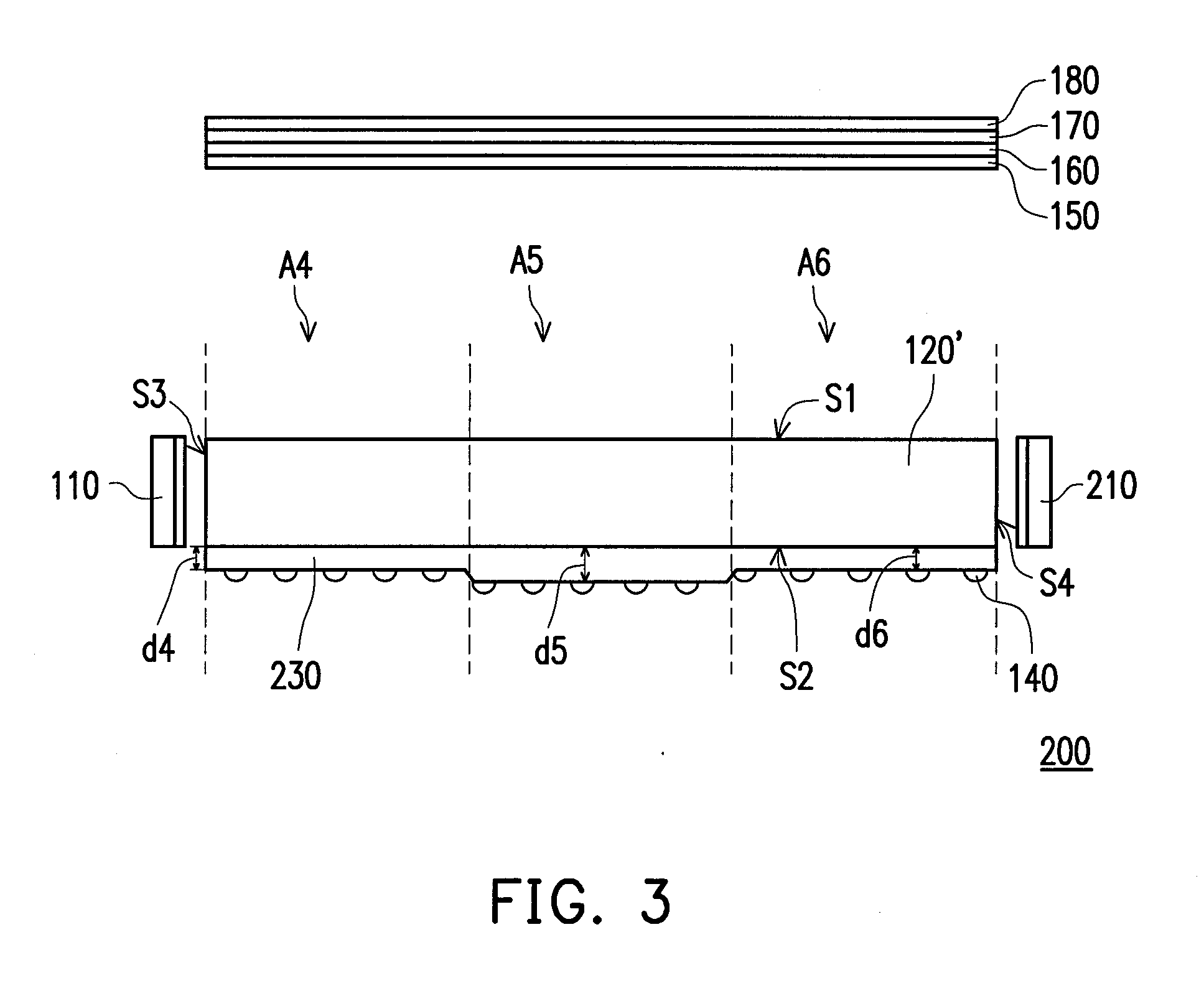
[0038]FIG. 3 is a schematic view illustrating a light source device according to a second embodiment of the invention. As indicated in FIG. 3, the light source device 200 is similar to the light source device 100 illustrated in FIG. 1, while the main difference between the light source devices 200 and 100 lies in that the light source device 200 further includes a light-emitting element 210, and the LGP 120′ further has a light-incident surface S4 opposite to the light-incident surface S3. The light-emitting element 210 is located beside the light-incident surface S4. In this embodiment, the light-emitting element 210 is a white LED, for instance.
[0039]The thickness of the optical thin film 230 close to the light-emitting elements 110 and 210 is less than the thickness of the optical thin film 230 away from the light-emitting elements 110 and 210. That is to say, the thickness d5 of the optical thin film 230 in the light-transmissive region A5 at the center of the LGP 120′ is greate...
PUM
 Abstract
Description
Claims
Application Information
 - R&D
- Intellectual Property
- Life Sciences
- Materials
- Tech Scout
- Unparalleled Data Quality
- Higher Quality Content
- 60% Fewer Hallucinations
Browse by: Latest US Patents, China's latest patents, Technical Efficacy Thesaurus, Application Domain, Technology Topic, Popular Technical Reports.
© 2025 PatSnap. All rights reserved.Legal|Privacy policy|Modern Slavery Act Transparency Statement|Sitemap|About US| Contact US: help@patsnap.com


