Semiconductor device and electroluminescent device and method of making the same
- Summary
- Abstract
- Description
- Claims
- Application Information
AI Technical Summary
Benefits of technology
Problems solved by technology
Method used
Image

Examples
Embodiment Construction
[0022]To provide a better understanding of the present invention, preferred embodiments will be made in detail. The preferred embodiments of the present invention are illustrated in the accompanying drawings with numbered elements.
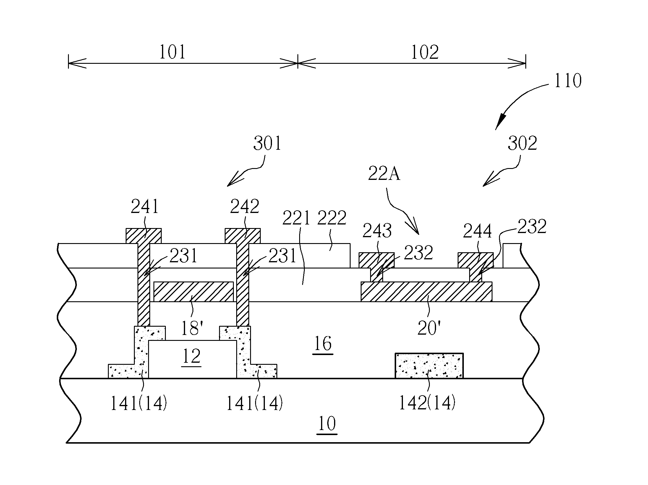
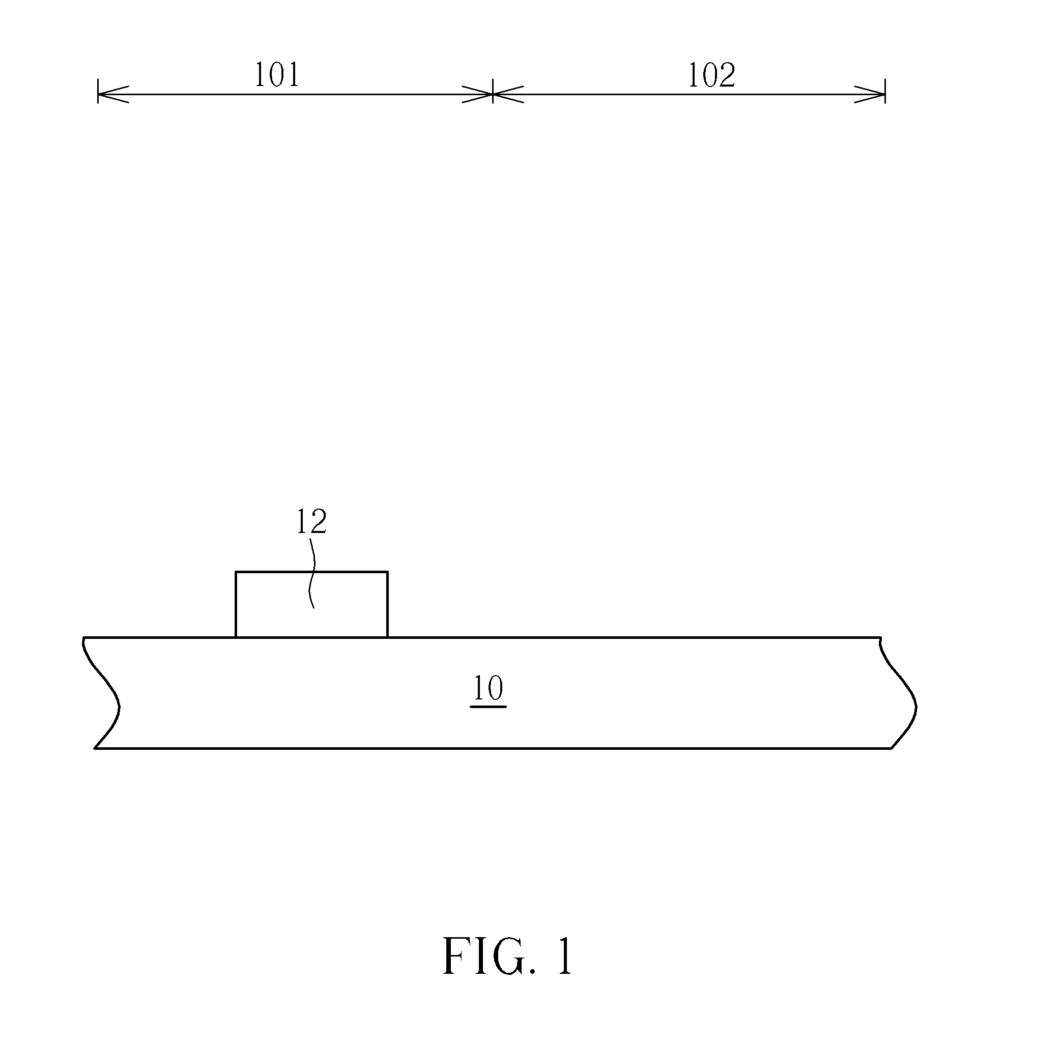
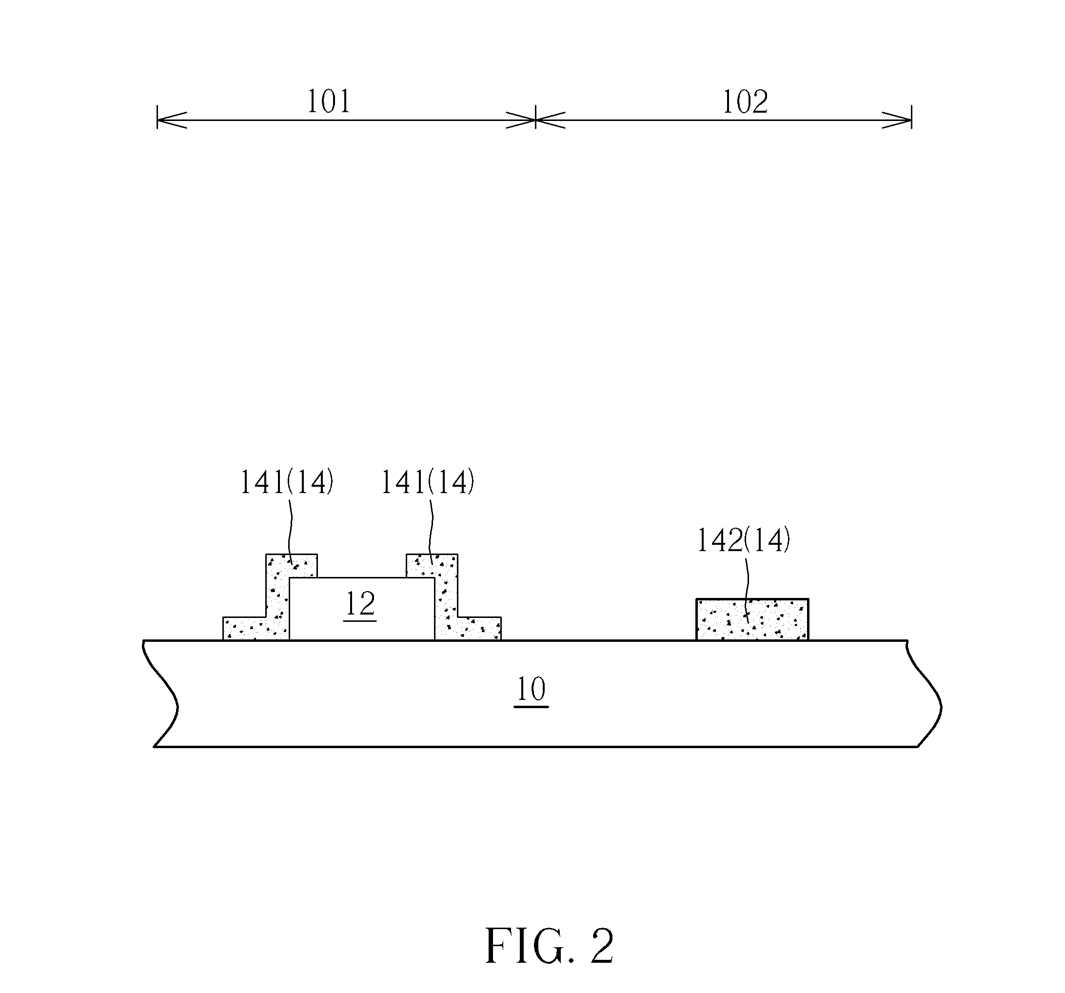
[0023]Please refer to FIGS. 1-4. FIGS. 1-4 are schematic diagrams illustrating a method for forming a semiconductor device according to a first preferred embodiment of the present invention. As shown in FIG. 1, a substrate 10 is first provided. The substrate 10 may be a transparent substrate e.g. a glass substrate, a plastic substrate or a quartz substrate, but not limited thereto. The substrate 10 has a first region 101 and a second region 102. The first region 101 is used to dispose a first thin film transistor (TFT) device, while the second region 102 is used to dispose a second TFT device. Subsequently, a first channel layer 12 is formed in the first region 101 of the substrate 10. In this embodiment, the first channel layer 12 is an amorphous silicon ...
PUM
 Abstract
Description
Claims
Application Information
 - R&D
- Intellectual Property
- Life Sciences
- Materials
- Tech Scout
- Unparalleled Data Quality
- Higher Quality Content
- 60% Fewer Hallucinations
Browse by: Latest US Patents, China's latest patents, Technical Efficacy Thesaurus, Application Domain, Technology Topic, Popular Technical Reports.
© 2025 PatSnap. All rights reserved.Legal|Privacy policy|Modern Slavery Act Transparency Statement|Sitemap|About US| Contact US: help@patsnap.com