
Electronic component mounting device and an operation performing method for mounting electronic components

a technology for electronic components and mounting devices, which is applied in the direction of metal working apparatus, metal-working machine components, manufacturing tools, etc., can solve the problems of long height measurement time, inability to ensure good operation quality, and inability to avoid significant productivity drop, so as to achieve high height precision and improve operation quality and productivity. , the effect of improving productivity

Active Publication Date: 2012-12-20
PANASONIC INTELLECTUAL PROPERTY MANAGEMENT CO LTD
View PDF6 Cites 17 Cited by
  • Summary
  • Abstract
  • Description
  • Claims
  • Application Information

AI Technical Summary

Benefits of technology

[0023]According to the present invention, the height precision division information that divide the height precision required for up and down movements of operating heads into the first division which indicates a normal height precision and the second division which indicates that a high height precision is required based on the type of electronic components are stored as operation data beforehand, and in the operation performing procedures, when the electronic component which is an operation object belongs to the first division, the operating head is made to move up and down based on an approximate operation position height derived from an approximate curved surface of the top surface of the board which is calculated by using the height measurement result obtained on a plurality of height measuring points on the top surface of the board, and when the electronic component which is an operation object belongs to the second division, the operating head is made to move up and down based on an individual operation position height obtained by individually measuring the board height at the operation position. Therefore, the operating head can be made to move up and down based on the precision to be required for the electronic component which is an object, and both the operation quality and the productivity can be improved.

Problems solved by technology

However, in the conventional art to approximate the warp deformation of the surface of the board with the curved surface model that is shown by a mathematical formula including the example shown in the above-mentioned patent document, due to the increase of precision level required for electronic components which are operation objects, the following problems occur.
However, because the curved surface model that is obtained by measuring the surface of the board beforehand is actually an approximate model obtained with a mathematical formula, when the model is applied to a real board having irregularity locally, the right operation height of the surface of the board is not shown as an operation position, and good operation quality cannot be secured.
Further, to prevent the defect due to local deformation of the board, it may be considered to perform height measurements individually for each of the operation positions corresponding to the respective electronic components, but when a large number of components are to be mounted on the board, a long time is needed for the height measurements, and a significant drop of the productivity cannot be avoided.
Thus, in the conventional electronic component mounting devices and operation performing methods for mounting electronic components, there is a problem that it is difficult to improve both the productivity and the operation quality such as the component mounting quality to and the resin coating quality.

Method used


Image

  • Electronic component mounting device and an operation performing method for mounting electronic components
  • Electronic component mounting device and an operation performing method for mounting electronic components
  • Electronic component mounting device and an operation performing method for mounting electronic components

Examples


Embodiment Construction

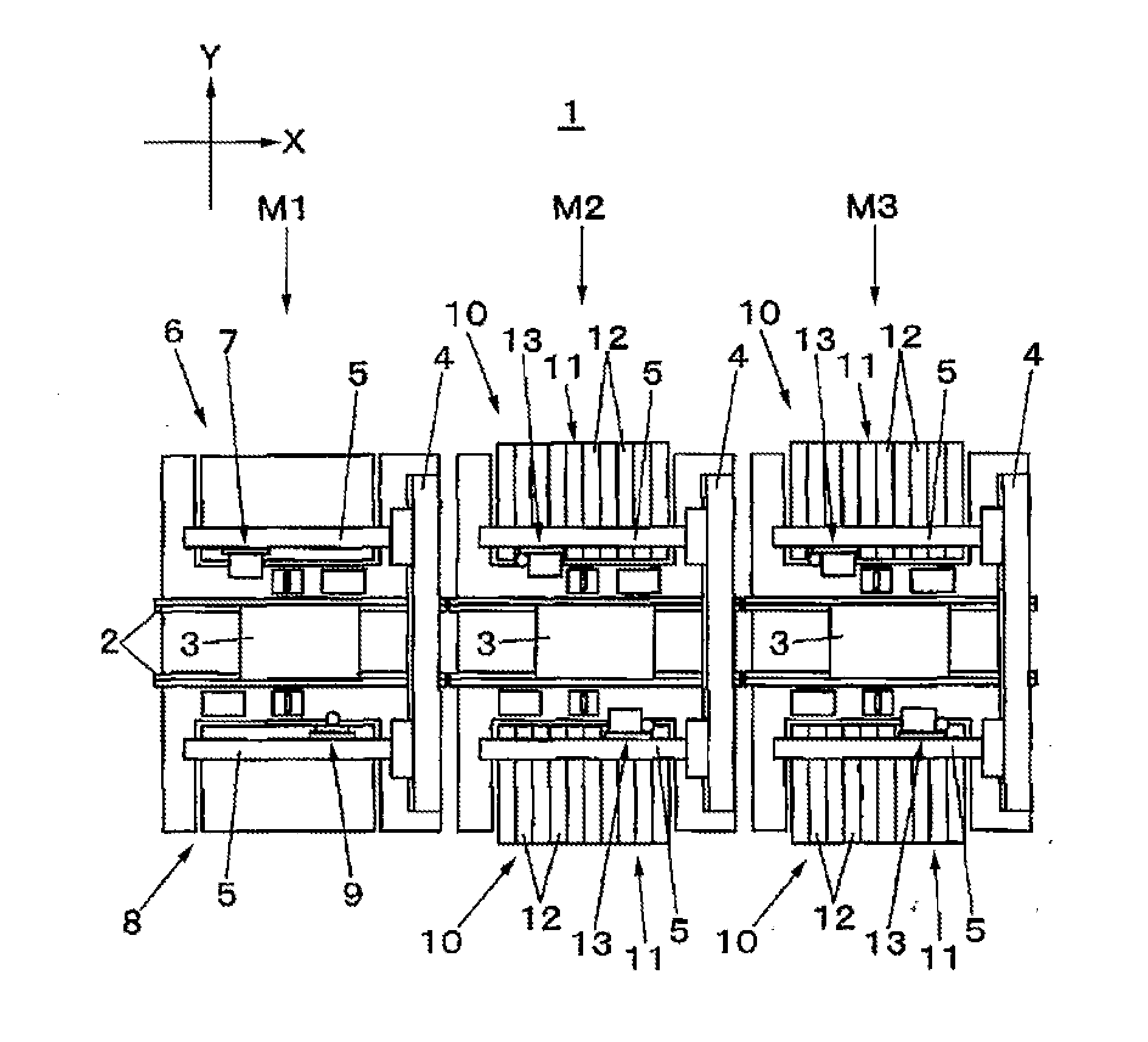
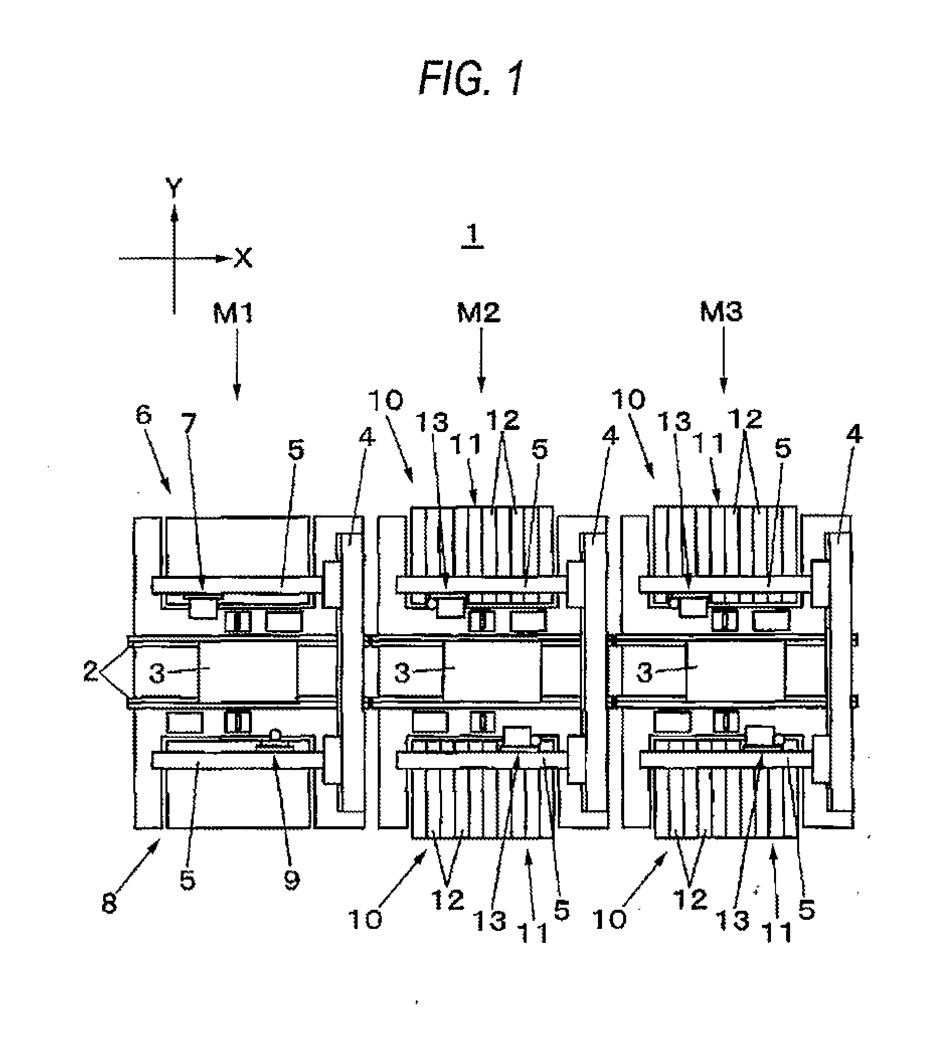
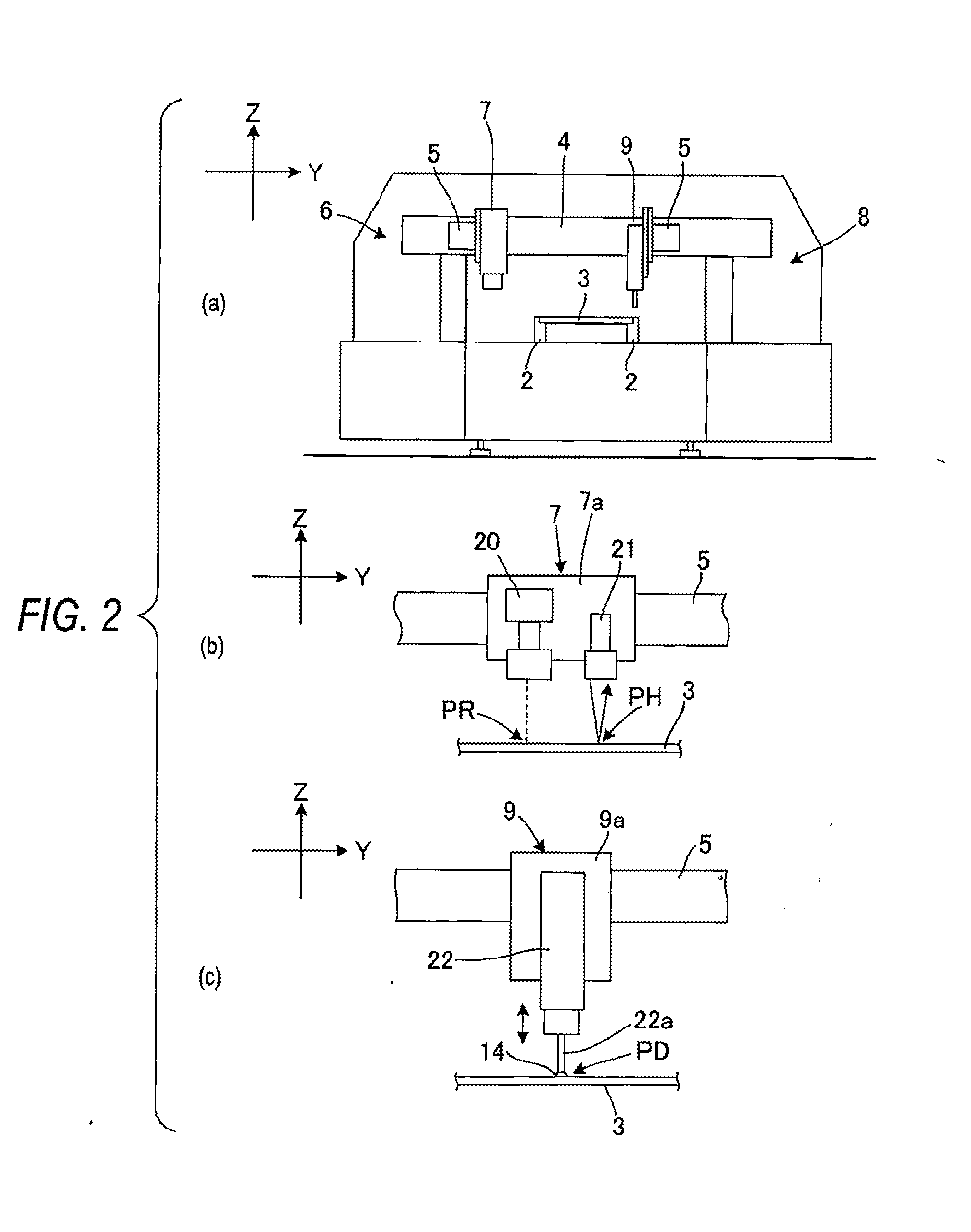
[0033]At first, a structure of an electronic component mounting line 1 is described with reference to FIG. 1. The electronic component mounting line 1 is formed by coupling a plurality of electronic component mounting devices (M1, M2 and M3) in series. These devices have functions of performing predetermined operations for mounting every electronic component on a board 3 on which the electronic components are to be mounted. Under the collective control of an administrative computer 30 (referring to FIG. 4), the respective devices sequentially perform operations for mounting components on the same board 3. In the electronic component mounting line 1, the board 3 on which paste for solder bonding is printed by an upstream device is imported to the inspecting, measuring and coating device M1 located at an upstream position (left side in the figure). The board 3 is sequentially conveyed in the X direction (board conveying direction) of the electronic component mounting line 1, and becom...


PUM

PropertyMeasurementUnit
Heightaaaaaaaaaa

Abstract

It is intended to provide an electronic component mounting device and an operation performing method for mounting electronic components so that both the operation quality and the productivity can be improved. Height precision division information that divide the height precision required for up and down movements of operating heads into the first division which indicates a normal height precision and the second division which indicates that a high height precision is required based on the type of electronic components are stored as operation data beforehand. In operation performing procedures, when an electronic component belongs to the first division, an operating head is made to move up and down based on an approximate operation position height derived from an approximate curved surface of the top surface of a board which is calculated by using the height measurement result obtained by measuring a plurality of height measuring points on the surface of the board, and when the electronic component belongs to the second division, the operating head is made to move up and down based on an individual operation position height obtained by individually measuring the board height at the operation position.

Description

TECHNICAL FIELD [0001]The present invention relates to an electronic component mounting device which performs operations to mount electronic components on a board and an operation performing method for mounting electronic components on a board.BACKGROUND ART[0002]An electronic component mounting line that produces a mounted board by mounting electronic components on the board is formed by coupling together a plurality of electronic component mounting devices which have different operational functions, such as a coating device that coats a board with a viscous material like paste or adhesive that is used to bond electronic components with the board or a component mounting device that loads electronic components on a coated board. These electronic component mounting devices are configured so that predetermined electronic component mounting operations are performed by the respective electronic component mounting devices, such as a component loading operation and a viscous material coat...

Claims


Application Information

Patent Timeline
IPC IPC(8): H05K13/04H05K3/30
CPCH05K13/0413H05K13/0452Y10T29/53013Y10T29/4913Y10T29/49128Y10T29/49904Y10T29/53174Y10T29/53178H01L2224/81H05K13/0812H05K13/083H05K13/04
Inventor ENDO, TADASHIOGATA, HIROSHIKIMURA, TOMOHIROYOKOI, TAKAAKI
Owner PANASONIC INTELLECTUAL PROPERTY MANAGEMENT CO LTD
Learn More