
Pixel Structure and a Driving Method Thereof

a driving method and pixel technology, applied in the field of pixel structure and driving method thereof, can solve the problems of color washout, invalid charging duration to be reduced to half the original one, and the kind of technology cannot be implemented in an lcd having a higher frame rate, so as to reduce manufacturing costs

Active Publication Date: 2012-11-01
SHENZHEN CHINA STAR OPTOELECTRONICS TECH CO LTD
View PDF3 Cites 7 Cited by
  • Summary
  • Abstract
  • Description
  • Claims
  • Application Information

AI Technical Summary

Benefits of technology

[0012]An object of the present invention is to provide a pixel structure where no additional gamma circuit needs to be disposed for minimizing color washout and a driving method thereof, and further to reduce manufacturing cost due to an additional gamma circuit used in the conventional technology.
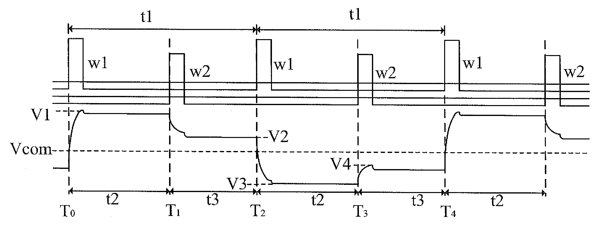
[0019]In contrast to the prior art, the pixel structure comprises two TFTs, an LC capacitor, a first storage capacitor, and a second storage capacitor according to the present invention. The two TFTs are connected to two scan lines, respectively, for conducting at different timings. When conducting, one of the TFTs stores data voltage applied on the data line into the first storage capacitor and into the LC capacitor. While the other TFT conducts, it conducts the first storage capacitor and second storage capacitor, allowing the first and second storage capacitors to perform charge sharing. Owing to the driving method, the difference in voltage between the LC capacitor and common voltage is reduced from charge sharing and further, a color washout effect of the panel is minimized.

Problems solved by technology

Although the MVA technology can be implemented on TFT-LCDs to make the TFT-LCDs with a wide viewing angle, a problem of color washout occurs, which is blamed by the public.
Obviously, the method has a problem of doubling the number of the scan lines, causing the valid charging duration to be reduced to half the original one.
Thus, such kind of technology is unable to be implemented in an LCD having a higher frame rate due to insufficient charging duration.
An overall manufacturing cost of the circuit is increased due two gamma circuits used.

Method used


Image

  • Pixel Structure and a Driving Method Thereof
  • Pixel Structure and a Driving Method Thereof
  • Pixel Structure and a Driving Method Thereof

Examples


Embodiment Construction

[0028]Spatially relative terms, such as “beneath”, “below”, “lower”, “above”, “upper” and the like, may be used herein for ease of description to describe one element or feature's relationship to another element(s) or feature(s) as illustrated in the figures. It will be understood that the spatially relative terms are intended to encompass different orientations of the device in use or operation in addition to the orientation depicted in the figures.

[0029]Referring to FIG. 5, FIG. 5 is an equivalent circuit diagram of a pixel unit 700 according to an embodiment of the present invention. The pixel unit 700 comprises a first TFT S1, a second TFT S2, a first storage capacitor CST1, a second storage capacitor CST2, and an LC capacitor CLC. The first TFT S1 corresponds to a first scan line G1(m), and the second TFT S2 corresponds to a second scan line G2(m).

[0030]The first TFT S1 comprises a gate coupled to the first scan line G1(m), a source coupled to a data line D(n), and a drain coup...


PUM


Abstract

A pixel structure and its related driving method are proposed. The pixel structure comprises a first transistor, a second transistor, a liquid crystal capacitor, a first storage capacitor, and a second storage capacitor. The first transistor comprises a gate coupled to a first scan line, a source coupled to a data line, and a drain coupled to the first storage capacitor. The first transistor is used for conducting the data line and the first storage capacitor. The second transistor comprises a gate coupled to a second scan line, a source coupled to the first storage capacitor, and a drain coupled to the second storage capacitor. A first polarity voltage applied on the data line is stored into the first storage capacitor during a first time period which the first transistor is turned on. The first storage capacitor discharges due to a connection between the first capacitor and the second capacitor during a second time period which the second transistor is turned on. By using such driving method, the difference in voltage between the liquid crystal capacitor and a common voltage is reduced from charge sharing for improving a color washout effect of the LCD panel.

Description

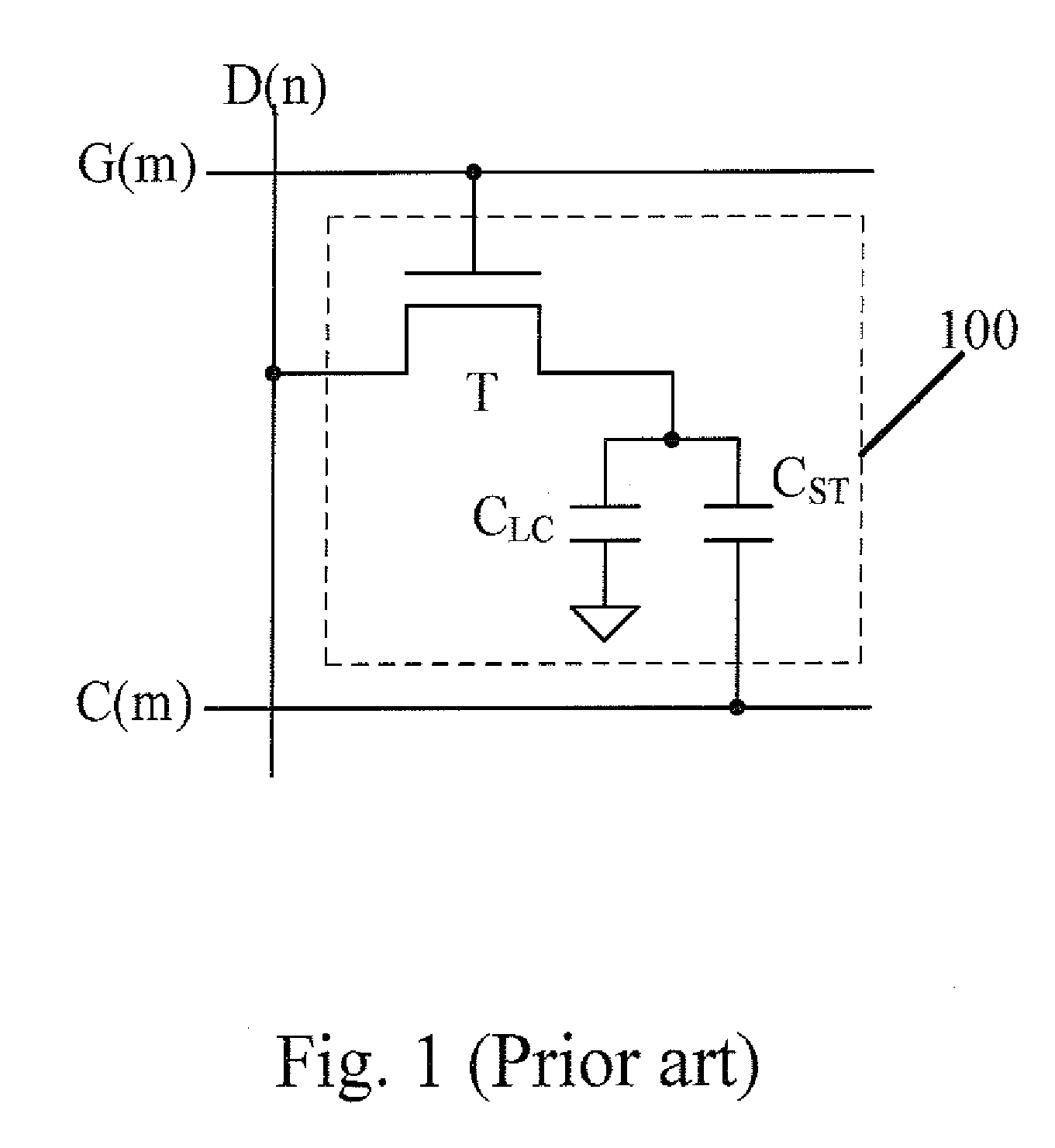
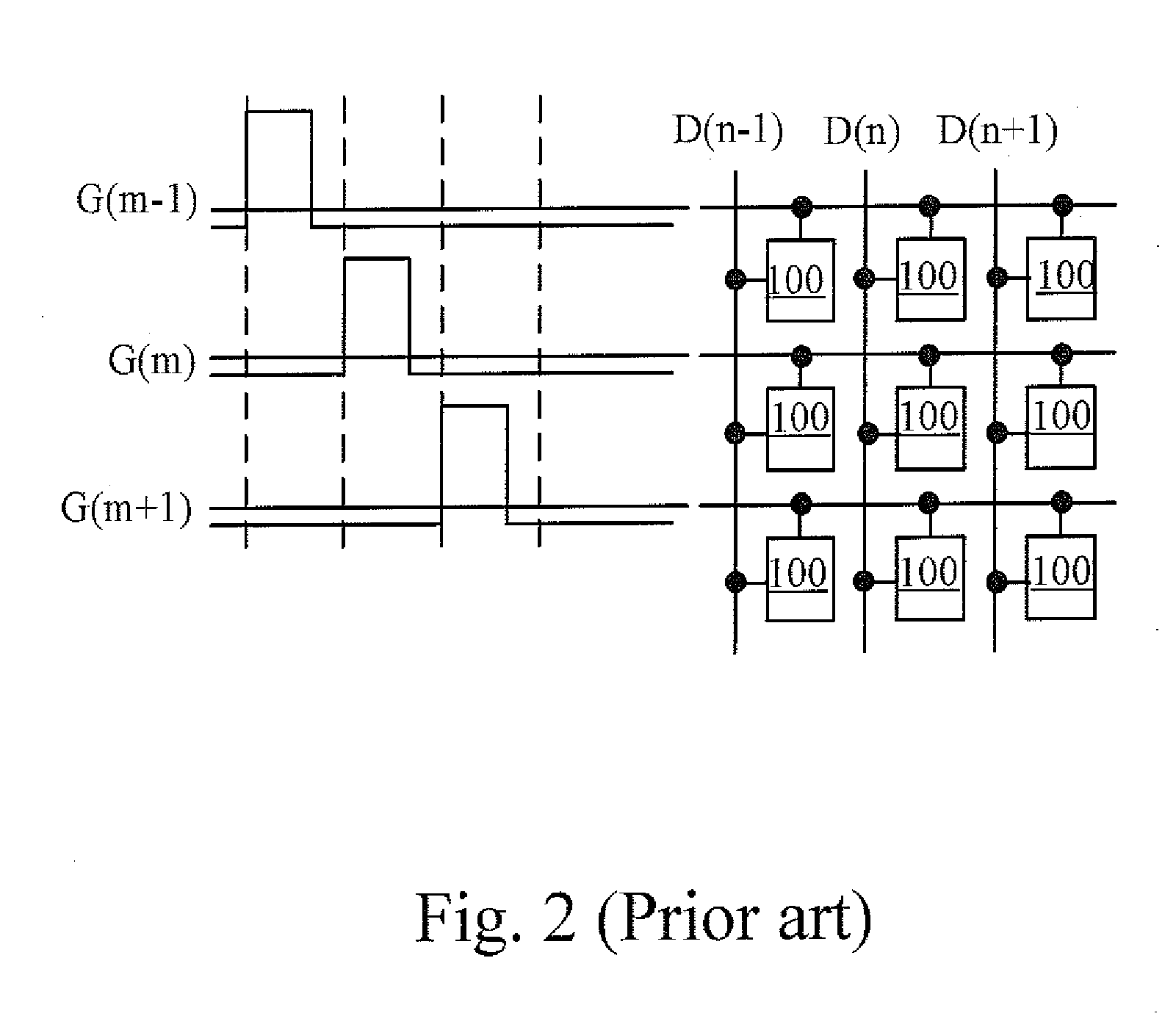
BACKGROUND OF THE INVENTION[0001]1. Field of the Invention[0002]The present invention relates to a pixel structure and a driving method thereof, and more particularly, to a pixel structure used to minimize color washout effect and a driving method thereof.[0003]2. Description of the Prior Art[0004]An advanced monitor with multiple functions is an important feature for use in current consumer electronic products. Liquid crystal displays (LCDs) which are colorful monitors with high resolution are widely used in various electronic products such as monitors for mobile phones, personal digital assistants (PDAs), digital cameras, laptop computers, and notebook computers.[0005]Thin-film-transistor liquid crystal displays (TFT-LCDs) have gradually become mainstream products in the consumer electronics market, for they have many merits such as high picture quality, efficient utilization of space, low consumption power, no radiation, etc. Referring to FIG. 1 showing an equivalent circuit diag...

Claims


Application Information

Patent Timeline
IPC IPC(8): G09G3/36G06F3/038
CPCG09G3/3659G09G2300/0447G09G2300/0814G09G3/36G09G2320/028G06F3/038G09G2300/0852
Inventor CHEN, CHENGHUNG
Owner SHENZHEN CHINA STAR OPTOELECTRONICS TECH CO LTD
Learn More