
Semiconductor device

a technology of semiconductor devices and liquid crystal display devices, which is applied in semiconductor devices, electrical devices, instruments, etc., can solve the problems of air bubbles generated by color filters and contamination of crystal layers, and achieve the effect of reducing the thickness and weight of the whole liquid crystal display devi

Active Publication Date: 2012-09-13
SEMICON ENERGY LAB CO LTD
View PDF2 Cites 6 Cited by
  • Summary
  • Abstract
  • Description
  • Claims
  • Application Information

AI Technical Summary

Benefits of technology

[0012]It is an object of the present invention to provide a liquid crystal display device that can achieve a wide viewing angle and high image display with high contrast. In particular, it is an object of the present invention to provide a liquid crystal display device that can achieve high display quality under external light.
[0017]It is to be noted that the fluorescent layer is luminous by external light as well as a backlight, and reduction in contrast is caused under external light; therefore, the fluorescent layer is not used. In order to improve contrast even under external light, a light interference layer is provided between the color filter and the first substrate in the present invention. The color filter comprises a black matrix and a colored layer; however, external light is reflected by a difference in refractive indices between the black matrix and the first substrate. The light interference layer is particularly effective in a case of using a chromium film as the black matrix. Even when the black matrix comprises a black resin, there is a difference in refractive indices between the black matrix and the first substrate. Also, there is also a difference in refractive indices between the colored layer and the first substrate. Therefore, external light is slightly reflected. For example, a refractive index of a glass substrate is approximately 1.5. While, a refractive index of the colored layer in a case of averaging each layer is approximately 1.6; however, there is a refractive index of approximately 1.8 depending on materials. Furthermore, when the light interference layer is provided between the color filter and the first substrate, a difference in the refractive indices is moderated, and light reflection can be further reduced.
[0018]The light interference layer may have a single layer or a multilayer as long as light reflection due to the black matrix or the colored layer can be prevented, and specifically, a layer that is referred to as an antireflection (preventing reflection) film is used. In addition, as the light interference layer, a dielectric multilayer film can be used. The dielectric multilayer film has a structure in which a low refractive index thin film and a high refractive index thin film are stacked.
[0027]According to the present invention, a liquid crystal display device capable of having a wide viewing angle and high image display with high contrast can be achieved. In particular, high contrast can be achieved under external light.
[0028]Further, one polarizing element having dichroism and a color filter are arranged on an inner side of a pair of glass substrates, and then one of the pair of the glass substrates can have a surface that is exposed. When the glass substrate surface is exposed, a protection film for preventing scratches on the glass substrate surface, an antireflection film for preventing glare of external light, an antistatic film for preventing attachment of dust, or an antiglare (prevention of dazzle) film can be easily attached thereto. It is to be noted that another polarizing element having dichroism is attached on an outer side of the other glass substrate that is not exposed.
[0030]Furthermore, when a plastic substrate or a hybrid substrate using a norbornene resin is used instead of the glass substrate, the thickness and weight of the whole liquid crystal display device can be further reduced.

Problems solved by technology

If the color filter and the liquid crystal layer are adjacent to each other, there is a risk that air bubbles are generated from the color filter or that the liquid crystal layer is contaminated with an impurity from the color filter.

Method used


Image

  • Semiconductor device
  • Semiconductor device
  • Semiconductor device

Examples


embodiment mode 1

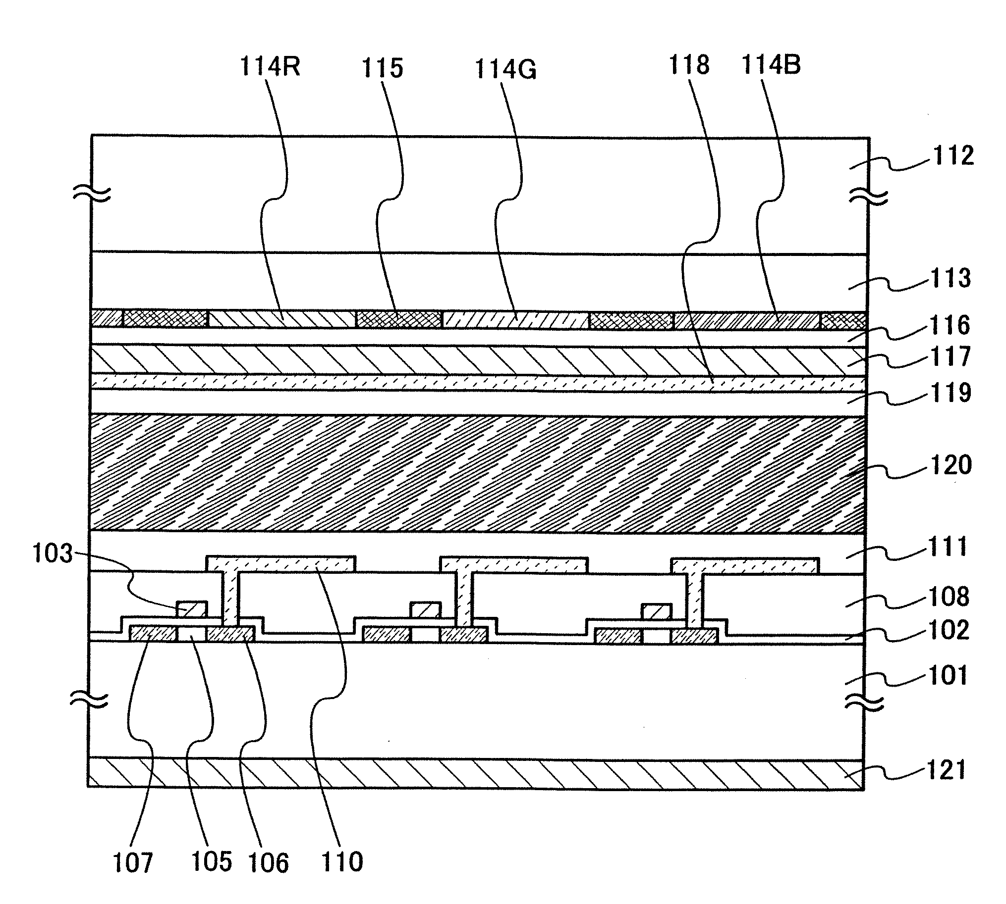
[0038]Here, an example of manufacturing a direct-view-type liquid crystal display device using TN (Twisted nematic) type liquid crystal with reference to FIG. 1.

[0039]First, a light interference layer 113 is formed over one surface of a first substrate 112 that is to be an opposite substrate. As the first substrate 112, a glass substrate is used.

[0040]The light interference layer 113 is provided to reduce reflection of external light at an interface that is formed from materials having different refractive indices. When the light interference layer 113 has a multilayer structure in which layers each having a different refractive index are stacked so that the interference layer 113 is widely effective to a wavelength region of visible light, external light reflected at interfaces of the stacked layers interferes and be canceled with each other; therefore, antireflection effect can be obtained. Here, the light interference layer 113 reduces reflection of external light at an interface...

embodiment mode 2

[0067]Although an example of the TN-type liquid crystal display device is shown in Embodiment Mode 1, in this embodiment mode, an example of an IPS (In Plane Switching) type liquid crystal display device is shown in FIG. 2. This IPS-type liquid crystal display device has a method in which a pixel electrode and a common electrode are formed over one of a pair of substrates that sandwich liquid crystal, and liquid crystal molecules are rotated in a plane between these electrodes, which is approximately parallel to a substrate surface, whereby switching of light is performed, and then display is performed. Since the liquid crystal molecules are rotated in an approximate parallel plane, inversions of gradation and hue are not generated due to a viewing angle, and accordingly, a wide viewing angle can be obtained as compared with the TN-type liquid crystal display device. In the IPS-type liquid crystal display device, arrangement of polarizing elements having dichroism is different from ...

embodiment 1

[0093]In this embodiment, an example in which the liquid crystal panel that is obtained in Embodiment Mode 1 or Embodiment Mode 2 is a liquid crystal module is shown in FIG. 3.

[0094]FIG. 3 is an explored perspective view of the liquid crystal module in which an LED (light emitting diode) is used as backlight. In a liquid crystal panel 302 obtained in Embodiment Mode 1 or Embodiment Mode 2, a plurality of driving ICs 305 are provided over an element substrate, and an FPC 307 that is electrically connected to a terminal provided over the element substrate is also provided.

[0095]A backlight 303 is arranged under the liquid crystal panel 302. In the backlight 303, a plurality of LEDs are used, and current is supplied from a connection code 306. As a light emitting material of the LED, an inorganic material or an organic material may be used.

[0096]It is to be noted that one kind of an LED that emits white light may be used, or three kinds of LEDs each of which emit red, blue, and green l...


PUM


Abstract

External light is reflected due to a difference in refractive indices of a black matrix and a glass substrate. When the black matrix is a black resin, there is a difference in refractive indices of the black resin and a first substrate. Also, there is a difference in refractive indices of the colored layer and the first substrate. Therefore, external light is slightly reflected. There is a problem in that the reflected light reduces contrast. A structure in which one polarizing element having dichroism is interposed between a pair of substrates is employed, and a light interference layer is provided between a color filter and a glass substrate, whereby a difference in refractive indices is moderated to reduce light reflection.

Description

BACKGROUND OF THE INVENTION[0001]1. Field of the Invention[0002]The present invention relates to a semiconductor device that has a circuit including a thin film transistor (hereinafter, referred to as a TFT) and a manufacturing method thereof. For example, the present invention relates to an electronic device on which an electro-optical device typified by a liquid crystal display panel is mounted as a component.[0003]It is to be noted that the term “semiconductor device” in the present specification indicates a general device capable of functioning by utilization of semiconductor characteristics, and electro-optic devices, semiconductor circuits, and electronic devices are all included in the semiconductor device.[0004]2. Description of the Related Art[0005]In recent years, a technique has attracted attention, in which a thin film transistor (TFT) is formed using a semiconductor thin film (a thickness of about several nm to several hundred nm) that is formed over a substrate having ...

Claims


Application Information

Patent Timeline
Patent Type & Authority Applications(United States)
IPC IPC(8): H01L27/15
CPCG02F1/133502G02F2001/133565G02F1/133784G02F1/133528G02F1/133565
Inventor ISHITANI, TETSUJIKUBOTA, DAISUKENISHI, TAKESHI
Owner SEMICON ENERGY LAB CO LTD
Learn More