Polycrystalline ferroelectric or multiferroic oxide articles on biaxially textured substrates and methods for making same
- Summary
- Abstract
- Description
- Claims
- Application Information
AI Technical Summary
Benefits of technology
Problems solved by technology
Method used
Image
Examples
examples
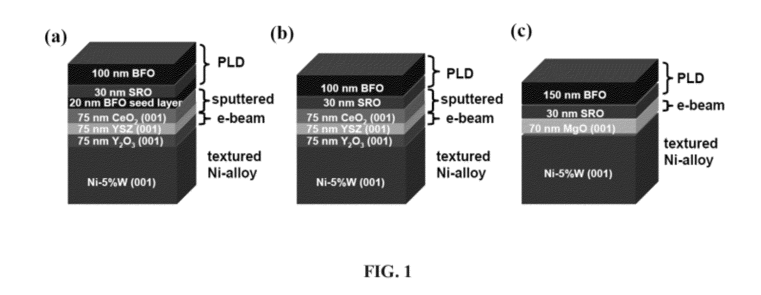
[0045]Highly oriented, polycrystalline BiFeO3 films were grown on rolling-assisted biaxially textured substrates (RABiTS) with a 30 nm thick SrRuO3 as a bottom electrode. The (111)- and (101)-oriented BiFeO3 films with 100 nm thickness were deposited by pulsed laser deposition (PLD) with a KrF laser (=248 nm) at a repetition rate of 10 Hz on SrRuO3-covered RABiTS which have the configuration CeO2 / YSZ / Y2O3 / Ni-3 at % W as used in superconductor applications [FIG. 1 (a) and (b)—identified as samples A and B]. In order to grow (111)-oriented BiFeO3 films, a 20 nm thick BiFeO3 seed layer was deposited followed by the SrRuO3 layer [FIG. 1 (a)]. A 150 nm thick (001)-oriented BiFeO3 film with a SrRuO3 bottom electrode was deposited by PLD on biaxially textured Ni-3 at % W tape, with an epitaxial MgO layer for oxygen diffusion barrier grown by electron beam evaporation [FIG. 1 (c)—identified as sample C]. All BiFeO3 and SrRuO3 films by PLD were grown at 700° C. in 100 mTorr O2 with a laser e...
PUM
| Property | Measurement | Unit |
|---|---|---|
| Density | aaaaa | aaaaa |
| Ferroelectricity | aaaaa | aaaaa |
Abstract
Description
Claims
Application Information
 - R&D
- Intellectual Property
- Life Sciences
- Materials
- Tech Scout
- Unparalleled Data Quality
- Higher Quality Content
- 60% Fewer Hallucinations
Browse by: Latest US Patents, China's latest patents, Technical Efficacy Thesaurus, Application Domain, Technology Topic, Popular Technical Reports.
© 2025 PatSnap. All rights reserved.Legal|Privacy policy|Modern Slavery Act Transparency Statement|Sitemap|About US| Contact US: help@patsnap.com


