
Light Signal Transfer Device with Conductive Carbon Line

a light signal and conductive carbon technology, applied in the direction of semiconductor devices, electrical devices, nanotechnology, etc., can solve the problem that the photodiode's minimum area cannot offer good performance, and achieve the effect of improving the performance of the light signal transfer device, reducing the area of the channel, and increasing the photo reception area

Active Publication Date: 2012-08-09
TAIWAN SEMICON MFG CO LTD
View PDF8 Cites 5 Cited by
  • Summary
  • Abstract
  • Description
  • Claims
  • Application Information

AI Technical Summary

Benefits of technology

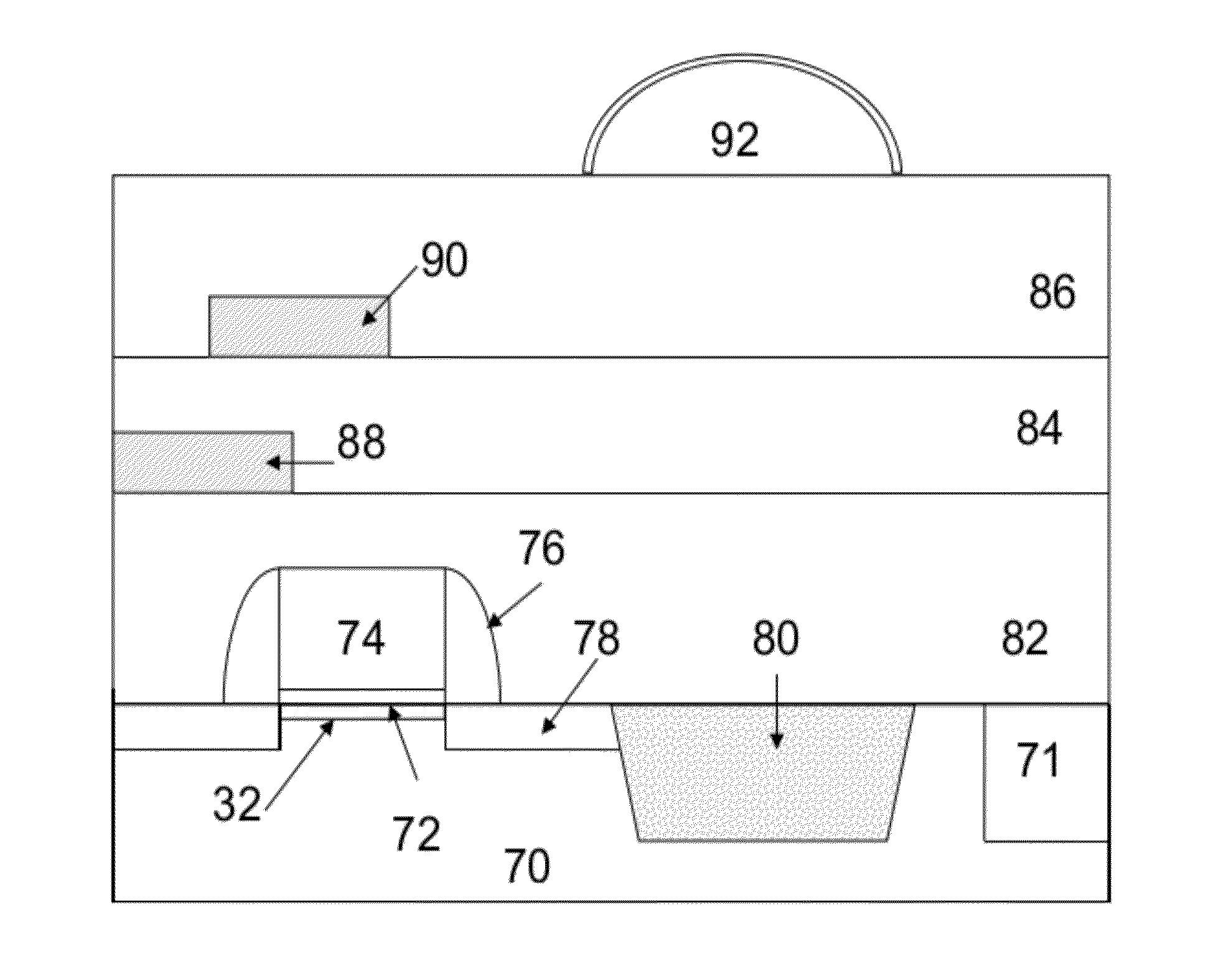
[0004]A light signal transfer device comprises a substrate having a gate dielectric layer; a source and drain doped regions formed in the substrate; a gate formed on the gate dielectric layer; a carbon nano-tube material formed under the gate dielectric layer to act a channel; and a photo-diode doped region formed adjacent to one of the source and drain doped regions, wherein the areas of the channel and the photo-diode doped region are fix, the carbon nano-tube material reducing area of the channel and increase photo reception area for the photo-diode doped region to improve performance of the light signal transfer device. Pluralities of isolation layers laminated over the light signal transfer device and at least one conductive pattern formed there between. The conductive pattern is formed with carbon nano-tube or conductive polymer. A lens is formed over the pluralities of isolation layers to guide incident light into the photo-diode doped region.
[0005]A light signal transfer device comprises a substrate having a gate formed in the substrate; a gate dielectric layer formed over the gate; a carbon nano-tube material formed over the gate dielectric layer to act a channel; a source and drain doped regions formed over the substrate and formed adjacent to the carbon nano-tube material; and a photo-diode doped region formed adjacent to one of the source and drain doped regions, wherein the areas of the channel and the photo-diode doped region are fix, the carbon nano-tube material reducing area of the channel and increase photo reception area for the photo-diode doped region to improve performance of the light signal transfer device.

Problems solved by technology

Thus, the minimized area of the photodiode cannot offer good performance.

Method used


Image

  • Light Signal Transfer Device with Conductive Carbon Line
  • Light Signal Transfer Device with Conductive Carbon Line
  • Light Signal Transfer Device with Conductive Carbon Line

Examples


Embodiment Construction

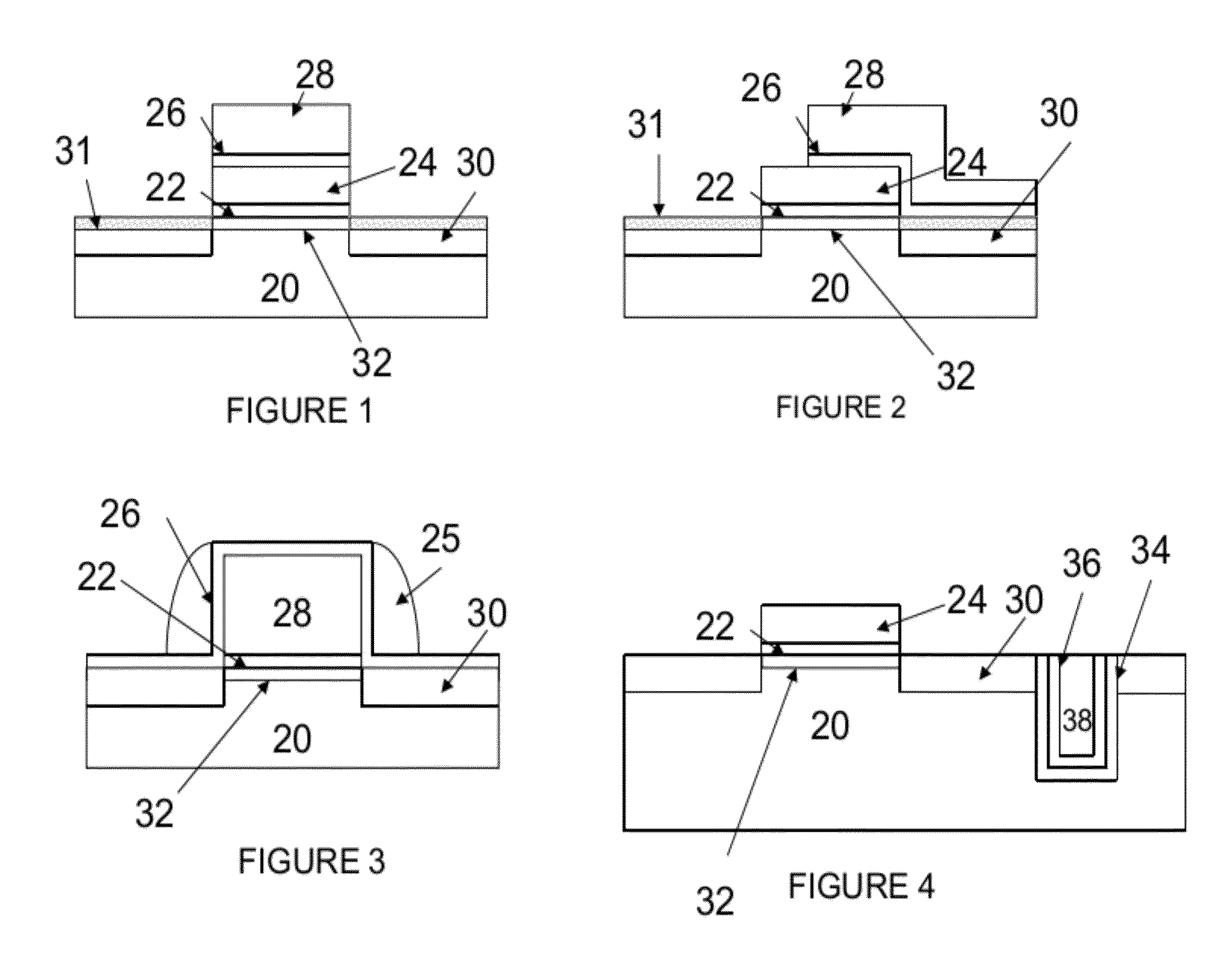
[0019]The present invention proposes a novel method to fabricate a memory. In the method, the operation speed for storing data can be increased by the cell structure. The detail description will be seen as follows. A semiconductor substrate is provided for the present invention. In a preferred embodiment, as shown in the FIG. 1, a single crystal silicon substrate 20 crystallographic orientation is provided. The substrate 20 includes a pattern of active areas comprising separated doped region such as the source / drain regions. A thin dielectric layer 22 is formed on the substrate 20 to act as gate dielectric layer. Typically, the dielectric layer 22 can be grown in oxygen ambient at a temperature of about 700 to 1100 degrees centigrade. Other method, such as chemical vapor deposition, can also form the oxide. Subsequently, a conductive layer 24 is formed on the oxide 22 to act the floating gate. The conductive layer 24 may be formed of doped polysilicon, in-situ doped polysilicon. For...


PUM


Abstract

A light signal transfer device comprises a substrate having a gate dielectric layer; a source and drain doped regions formed in the substrate; a gate formed on the gate dielectric layer; a carbon nano-tube material formed under the gate dielectric layer to act a channel; and a photo-diode doped region formed adjacent to one of the source and drain doped regions, wherein the areas of the channel and the photo-diode doped region are fixed, the carbon nano-tube material reducing area of the channel and increase photo reception area for the photo-diode doped region to improve performance of the light signal transfer device.

Description

CROSS-REFERENCE TO RELATED APPLICATION[0001]This application is a Continuation Application of an application Ser. No. 12 / 880,177, filed on Sep. 13, 2010, entitled “Liquid Crystal Panel with Conductive Carbon Line”, which is a divisional of an application Ser No. 12 / 076,928, filed on Mar. 25, 2008, entitled “Semiconductor Memory with Conductive Carbon”. The contents of the above-mentioned patent application is hereby incorporated by reference herein in its entirely and made a part of this specification.TECHNICAL FIELD[0002]The present invention relates to a light signal transfer device, and more specifically, to a light signal transfer device with conductive carbon (or conductive polymer) for channel.BACKGROUND OF THE RELATED ART[0003]A photodiode is a type of photodetector capable of converting light into either current or voltage, depending upon the mode of operation. Many diodes designed for use specifically as a photodiode use a PIN junction rather than a p-n junction, to increas...

Claims


Application Information

Patent Timeline
Patent Type & Authority Applications(United States)
IPC IPC(8): H01L31/112
CPCB82Y10/00H01L21/28273H01L21/28282H01L27/11521H01L27/11568H01L29/0665H01L29/7923H01L29/1033H01L29/66825H01L29/66833H01L29/78684H01L29/7881H01L29/792H01L29/0673H01L29/40114H01L29/40117H10B43/30H10B41/30
Inventor CHIANG, KUO-CHING
Owner TAIWAN SEMICON MFG CO LTD
Learn More