System for reducing sensor area in a back side illuminated CMOS active pixel sensor
a sensor and sensor array technology, applied in the field of backside illumination (bsi) imagers, can solve the problems of increasing the height of the column (i.e. increasing the size of the pixel array)
- Summary
- Abstract
- Description
- Claims
- Application Information
AI Technical Summary
Problems solved by technology
Method used
Image
Examples
Embodiment Construction
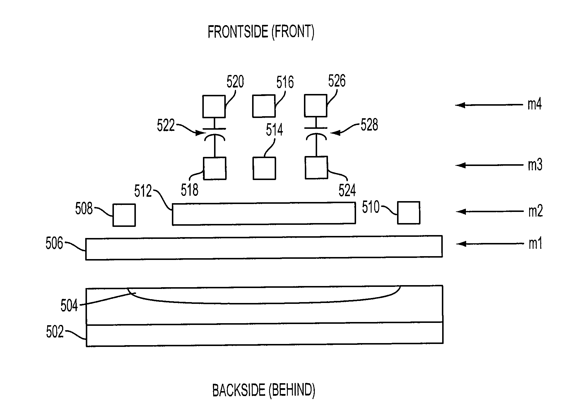
[0011]As will be described, the present invention provides a BSI imager implementing metal S / H parasitic capacitors on the front side (i.e. overlapping the pixels) of the BSI the pixel array. The present invention also provides a method of making the BSI imager. In general, the metal plate capacitors are positioned in a layer on the front side of the BSI imager along with the other wiring / conductors (i.e. pixel selection wires, pixel output wires, pixel power wires, etc.). The capacitors are positioned vertically, horizontally, or a combination of horizontally and vertically with respect to the pixel array. One benefit from this configuration is that a smaller imager (i.e. shorter column height) may be formed.
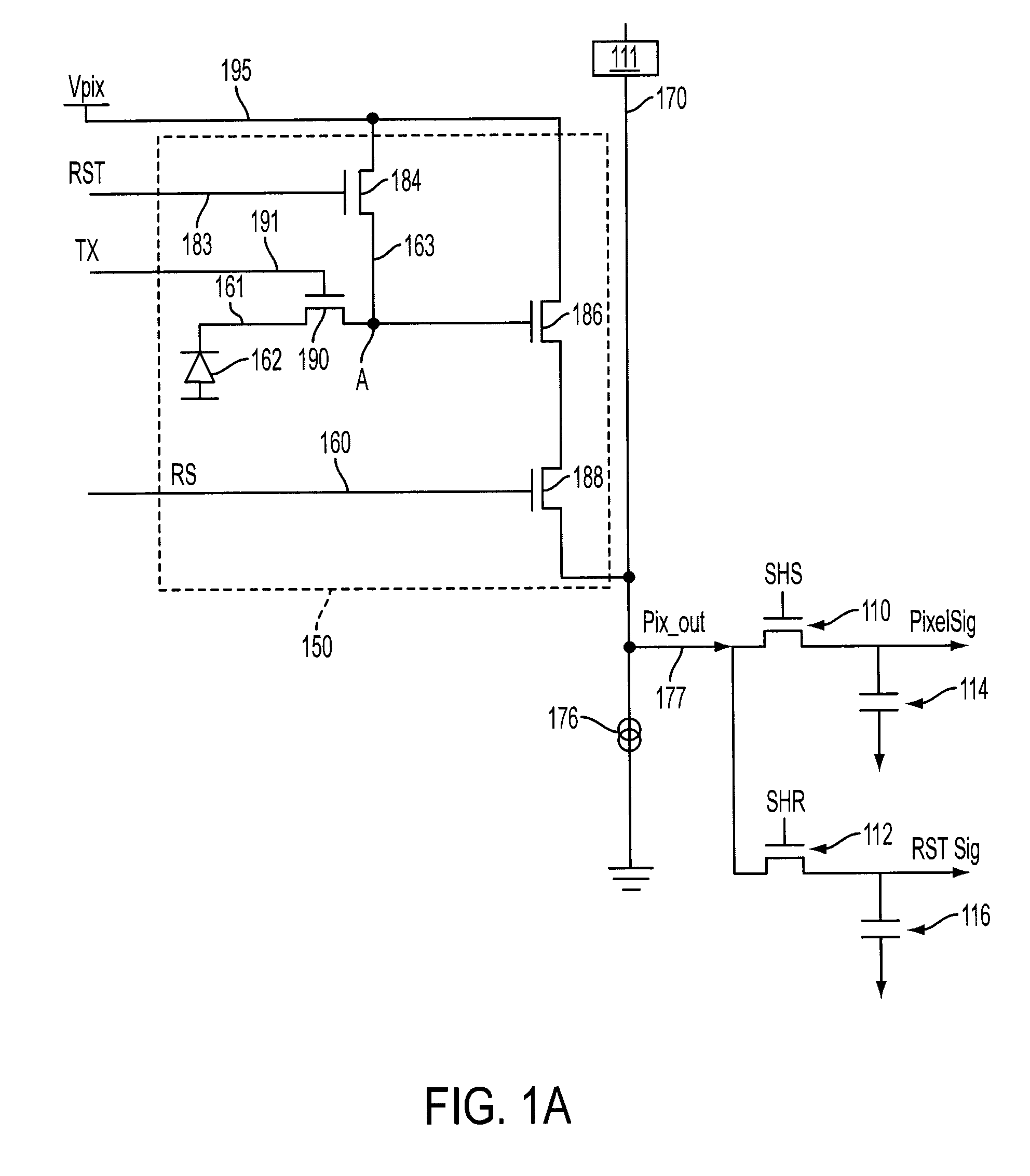
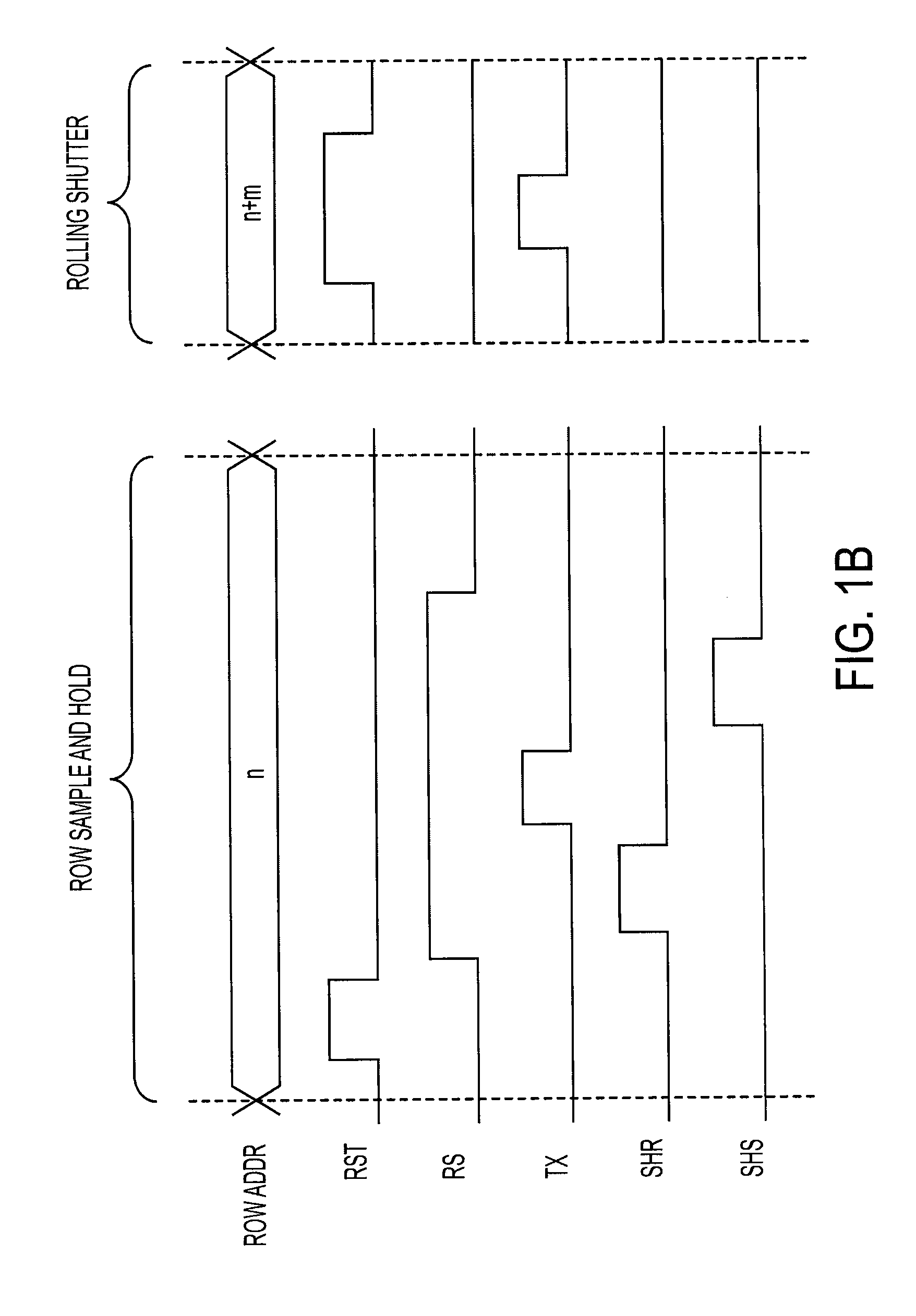
[0012]A conventional four transistor (4T) circuit for a pixel 150 of a CMOS imager is illustrated in FIG. 1A. Pixel 150 is a 4T pixel, where 4T is commonly used in the art to designate use of four transistors to operate the pixel. The 4T pixel 150 has a photo-sensor such as a p...
PUM
 Abstract
Description
Claims
Application Information
 - R&D
- Intellectual Property
- Life Sciences
- Materials
- Tech Scout
- Unparalleled Data Quality
- Higher Quality Content
- 60% Fewer Hallucinations
Browse by: Latest US Patents, China's latest patents, Technical Efficacy Thesaurus, Application Domain, Technology Topic, Popular Technical Reports.
© 2025 PatSnap. All rights reserved.Legal|Privacy policy|Modern Slavery Act Transparency Statement|Sitemap|About US| Contact US: help@patsnap.com


