Output timing control circuit and semiconductor apparatus using the same

a timing control circuit and output data technology, applied in the field of output timing control circuit and semiconductor apparatus using the same, can solve the problems of deteriorating timing margin required when controlling output data, data may not be received correctly, and output data may not be able to be analyzed correctly

Active Publication Date: 2012-06-07
SK HYNIX INC
View PDF2 Cites 19 Cited by
  • Summary
  • Abstract
  • Description
  • Claims
  • Application Information

AI Technical Summary

Benefits of technology

[0011]In an embodiment of the present invention, an output timing control circuit of a semiconductor apparatus includes: a delay amount counter block configured to count a delay amount of an output reset pulse signal based on an external clock signal and output a first counting code, wherein the delay amount counter block is configured to control the delay amount of the output reset pulse signal depending upon a frequency of the external clock signal; an operation block configured to subtract a code value of the first counting code from a code value of a data output delay code, and output a delay control code; and a phase control block configured to control a phase of a read command signal by the number of clocks of a DLL clock signal corresponding to a code value of the delay control code, and output an output enable flag signal.
[0012]In an embodiment of the present invention, a semiconductor apparatus includes: a variable delay unit configured to control a delay amount of an external clock signal under the control of a phase detection signal, and

Problems solved by technology

Since a signal transmitted from a transmitter, e.g., a semiconductor memory apparatus may be affected by an environment, if data affected by the environment is transmitted from the transmitter without a clock which may be adjusted according to the env

Method used


Image

  • Output timing control circuit and semiconductor apparatus using the same
  • Output timing control circuit and semiconductor apparatus using the same
  • Output timing control circuit and semiconductor apparatus using the same

Examples


Embodiment Construction

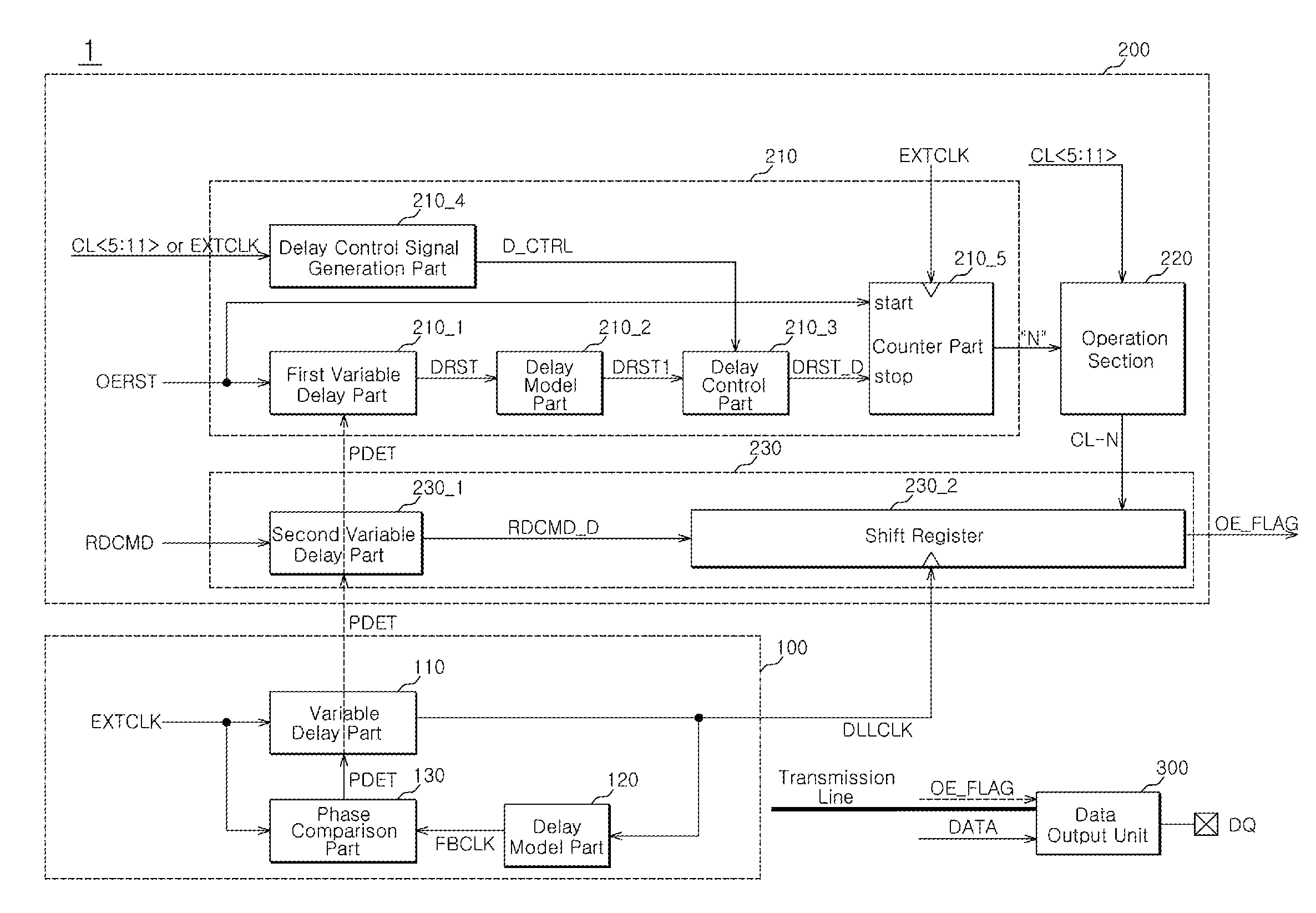
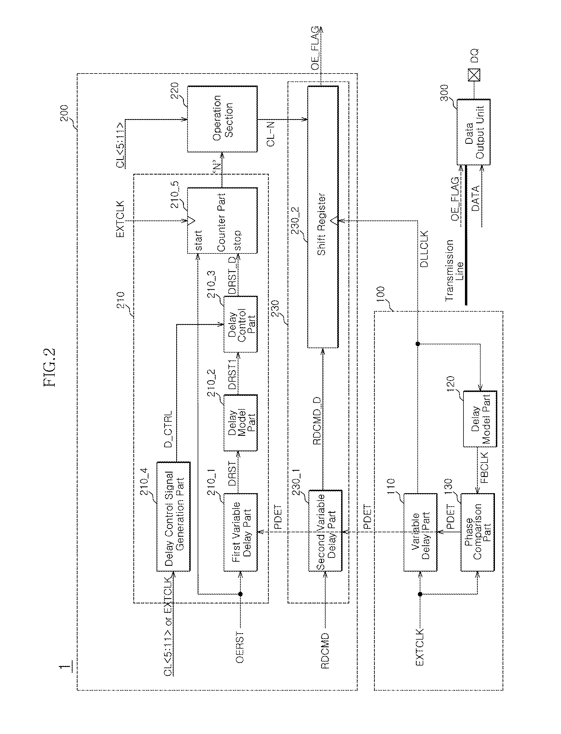
[0018]Hereinafter, an output timing control circuit and a semiconductor apparatus using the same according to the present invention will be described below with reference to the accompanying drawings through exemplary embodiments.

[0019]For reference, since terms, symbols and signs that are used in drawings and in this detailed description to designate devices, blocks, and so on may be used for detailed units as the occasion demands, it is to be noted that the same terms, symbols and signs may not designate the same devices, blocks, and so on in an entire circuitry.

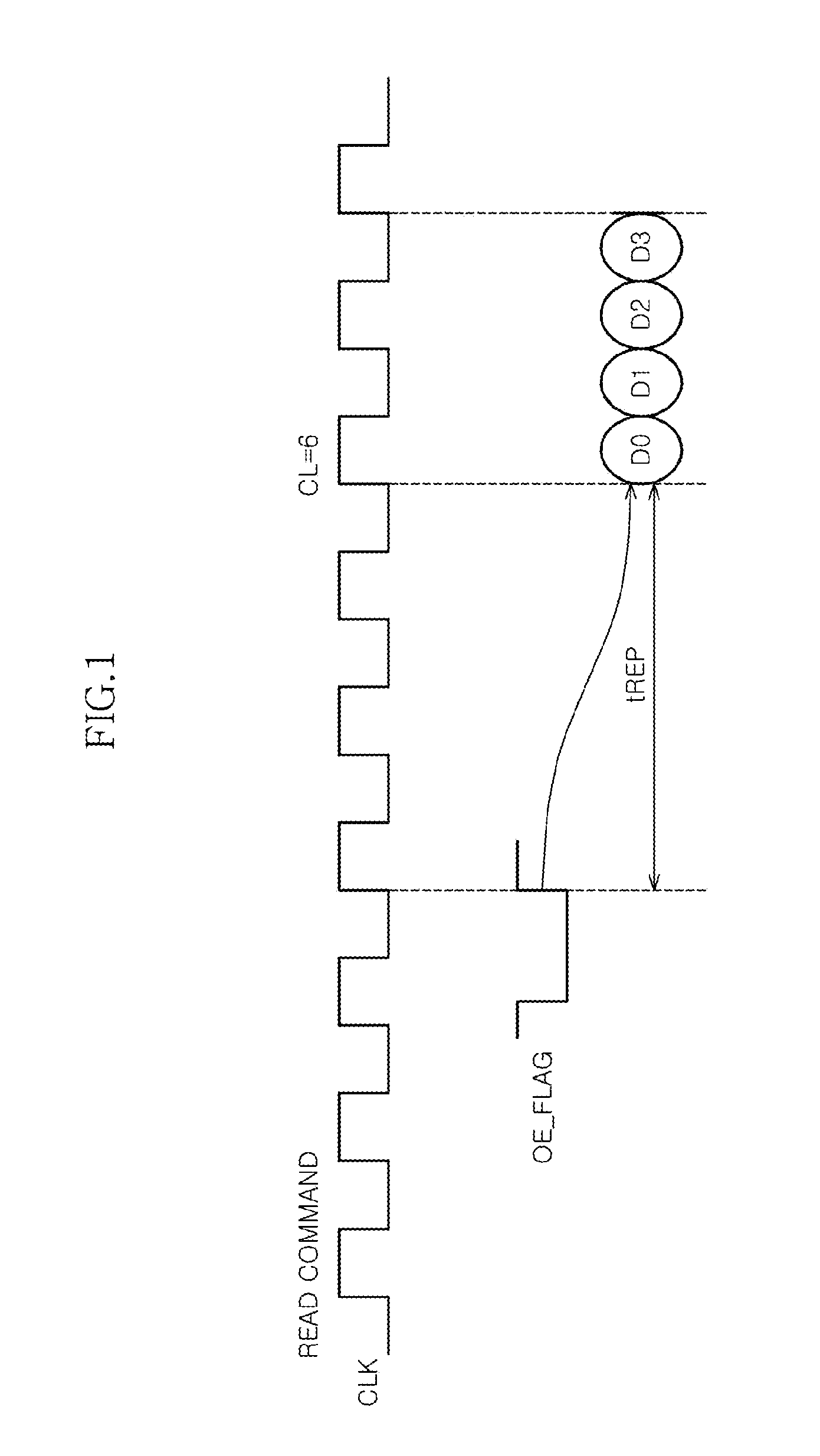
[0020]FIG. 1 is a timing diagram showing a timing at which output data is outputted according to data output delay information.

[0021]Referring to FIG. 1, an activation timing of an output enable flag signal OE_FLAG, on which data output delay information is reflected, is advanced by a model delay value tREP from a time at which output data is to be outputted. Further, the activation timing of the output enable flag signal ...


PUM


Abstract

An output timing control circuit of a semiconductor apparatus includes a delay amount counter block configured to count a delay amount of an output reset pulse signal based on an external clock signal and output a first counting code, wherein the delay amount counter block is configured to control the delay amount of the output reset pulse signal depending upon a frequency of the external clock signal; an operation block configured to subtract a code value of the first counting code from a code value of a data output delay code, and output a delay control code; and a phase control block configured to control a phase of a read command signal by the number of clocks of a DLL clock signal corresponding to a code value of the delay control code, and output an output enable flag signal.

Description

CROSS-REFERENCES TO RELATED APPLICATION[0001]The present application claims priority under 35 U.S.C. §119(a) to Korean application number 10-2010-0124197, filed on Dec. 7, 2010, in the Korean Intellectual Property Office, which is incorporated herein by reference in its entirety.BACKGROUND[0002]1. Technical Field[0003]The present invention relates generally to a semiconductor apparatus, and more particularly, to a technology for controlling an output timing of output data according to data output delay information.[0004]2. Related Art[0005]A semiconductor apparatus operates in synchronization with a reference periodic pulse signal such as a clock, in order to increase an operation speed and ensure an efficient internal operation. Accordingly, most semiconductor apparatuses operate using a clock supplied form an outside or an internal clock generated therein.[0006]Since a signal transmitted from a transmitter, e.g., a semiconductor memory apparatus may be affected by an environment, ...

Claims


Application Information

Patent Timeline
IPC IPC(8): G06M3/02
CPCH03K5/131
Inventor CHOI, HOON
Owner SK HYNIX INC
Why Eureka
Try Eureka