
Gallium nitride LED devices with pitted layers and methods for making thereof

a technology of gallium nitride led devices and pitted layers, which is applied in the direction of semiconductor/solid-state device manufacturing, semiconductor devices, electrical equipment, etc., can solve the problems of limited efficiency of conventional led devices, and achieve the effect of less fabrication time, high peak value of internal quantum efficiency and simple structur

Inactive Publication Date: 2012-05-24
PINECONE ENERGIES
View PDF0 Cites 15 Cited by
  • Summary
  • Abstract
  • Description
  • Claims
  • Application Information

AI Technical Summary

Benefits of technology

[0012]Many benefits are achieved by way of the present invention over conventional techniques. Some embodiments of the present invention provide a GaN LED structure that has a simpler structure than some conventional LED structures. Certain embodiments of the present invention provide a GaN LED structure that takes much less time to fabricate than certain conventional LED structures. Some embodiments of the present invention provide a GaN LED structure that achieves a high peak value for internal quantum efficiency by effectively using a pitted layer.

Problems solved by technology

But conventional LED devices often have limited efficiency; hence it is highly desirable to improve structures and fabrication techniques of LED devices.

Method used


Image

  • Gallium nitride LED devices with pitted layers and methods for making thereof
  • Gallium nitride LED devices with pitted layers and methods for making thereof
  • Gallium nitride LED devices with pitted layers and methods for making thereof

Examples


Embodiment Construction

[0023]The present invention is directed to semiconductor devices and fabrication methods. More particularly, the invention provides structures and methods using pitted layers in semiconductor devices. Merely by way of example, the invention has been applied to light-emitting diodes. But it would be recognized that the invention has a much broader range of applicability.

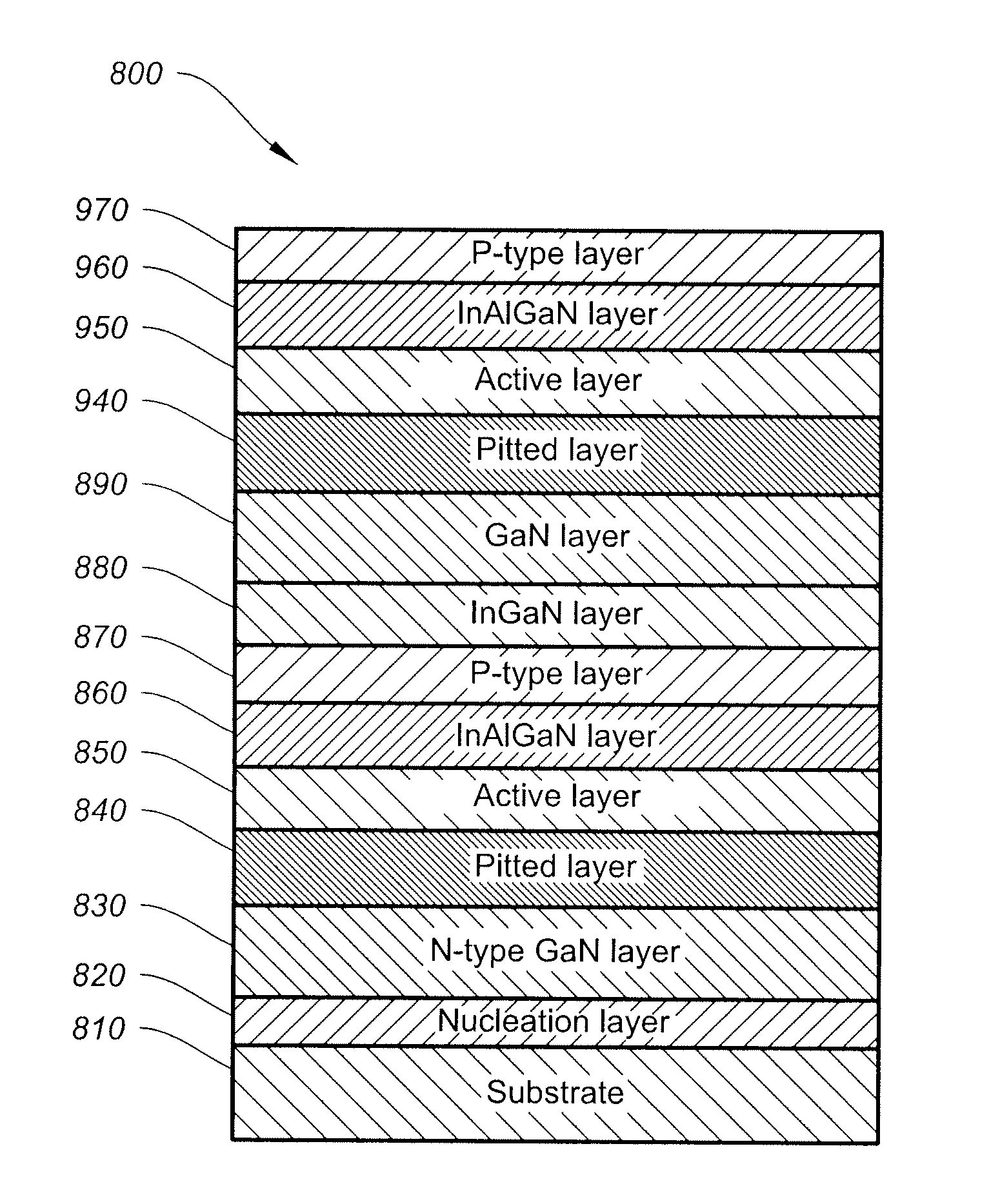
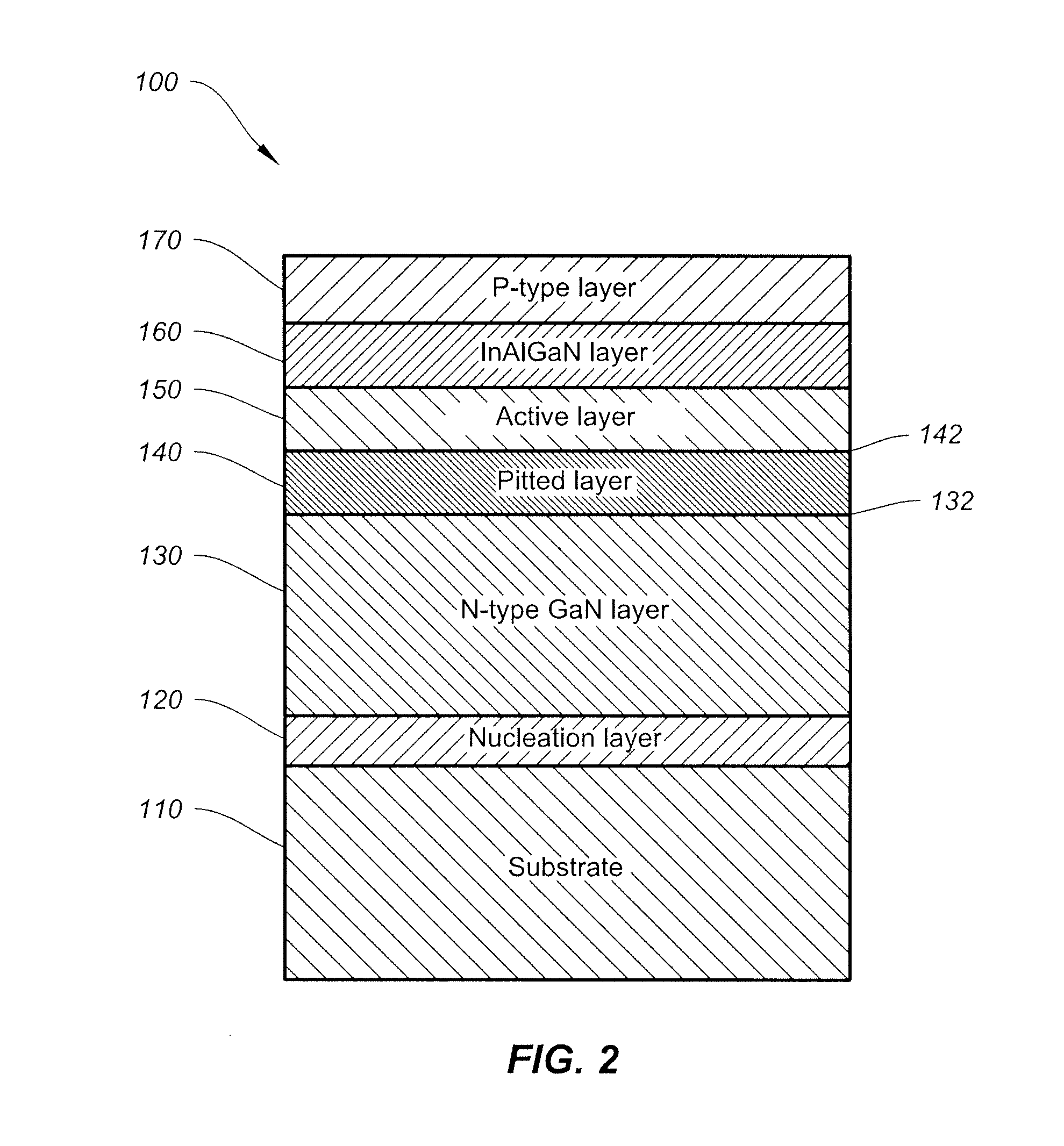
[0024]FIG. 2 is a simplified diagram showing a GaN LED structure with a pitted layer according to an embodiment of the present invention. This diagram is merely an example, which should not unduly limit the scope of the claims. One of ordinary skill in the art would recognize many variations, alternatives, and modifications. The GaN LED structure 100 includes a substrate 110, a nucleation layer 120, an n-type GaN layer 130, a pitted layer 140, an active layer 150, an InxAlyGazN layer 160, and a p-type layer 170. For example, x+y+z=1, 0≦x≦1, 0≦y≦1, and 0≦z≦1. In another example, the active layer 150 has a bandgap that ...


PUM


Abstract

Light-emitting diode device and method for making thereof. The device includes an n-type layer including a first surface and associated with a first thickness, and a pitted layer on the first surface. The pitted layer includes a second surface and associated with a second thickness ranging from 500 Å to 3000 Å. Additionally, the device includes an active layer on the second surface, the active layer being associated with a third thickness ranging from 10 Å to 20 Å, and a p-type layer on the active layer. The n-type layer is associated with a defect density at the first surface, and the defect density ranges from 1×109 cm−2 to 1×1010 cm−2. The pitted layer is associated with at least a plurality of pits.

Description

1. CROSS-REFERENCES TO RELATED APPLICATIONS[0001]This application claims priority to U.S. Provisional No. 61 / 416,634, filed Nov. 23, 2010, commonly assigned and incorporated by reference herein for all purposes.2. BACKGROUND OF THE INVENTION[0002]The present invention is directed to semiconductor devices and fabrication methods. More particularly, the invention provides structures and methods using pitted layers in semiconductor devices. Merely by way of example, the invention has been applied to light-emitting diodes. But it would be recognized that the invention has a much broader range of applicability.[0003]A light-emitting diode (LED) has been widely used as a light source. If the LED is forward biased, some electrons usually recombine with holes within the diode, thus emitting light. The color of the light often is determined by the energy gap that is associated with the LED. When used as a light source, the LED can provide significant advantages over incandescent light source...

Claims


Application Information

Patent Timeline
Patent Type & Authority Applications(United States)
IPC IPC(8): H01L33/06H01L33/58
CPCH01L21/0237H01L21/02458H01L21/02494H01L21/02507H01L21/02513H01L33/22H01L21/0262H01L21/02639H01L33/007H01L33/08H01L21/0254
Inventor LIU, HENG
Owner PINECONE ENERGIES
Learn More