
High Quality Factor Photonic Crystal Nanobeam Cavity and Method of Designing and Making Same

a photonic crystal and nanobeam technology, applied in the field of high quality factor photonic crystal nanobeam cavity and the field of designing and making same, can solve the problems of large loss caused by scattering due to imperfect design of the grating, inefficient trial-based method, etc., and achieve the effect of reducing modeling and computation tim

Active Publication Date: 2012-04-26
PRESIDENT & FELLOWS OF HARVARD COLLEGE
View PDF11 Cites 30 Cited by
  • Summary
  • Abstract
  • Description
  • Claims
  • Application Information

AI Technical Summary

Benefits of technology

The present invention is a method and device for designing and manufacturing a high-quality, ultrahigh Q, sub-wavelength scale nanobeam cavity with a resonance frequency that can be targeted for a specific application. This method reduces the time and computation required for designing and modeling the cavity, and it allows for the determination of the cavity's structure without fine tuning or resizing. The nanobeam cavity is based on optical strip waveguides with grating sections that provide constructive interference and produce optical resonance. The cavity has a plurality of grating sections with different filling fractions to create linearly increasing mirror strengths. The device can be used in various applications such as optical filters, sensors, and amplifiers.

Problems solved by technology

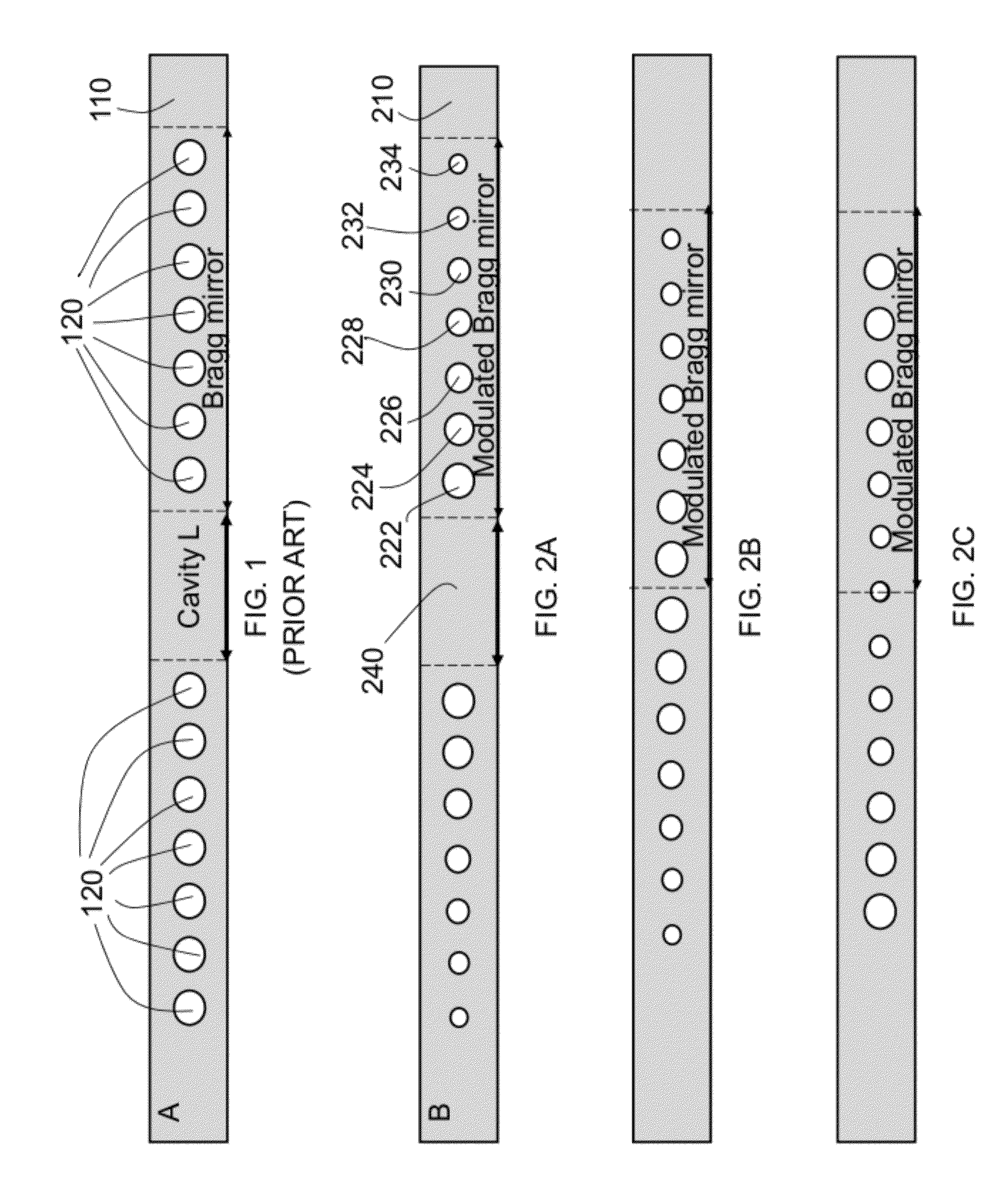
These grating sections provide constructive optical interference and confine light.
The major loss came from scattering due to imperfect design of the grating sections 120.
The large computational cost, in particular the computation time, needed to perform the simulation of high Q cavities makes such a trial-based method inefficient.

Method used


Image

  • High Quality Factor Photonic Crystal Nanobeam Cavity and Method of Designing and Making Same
  • High Quality Factor Photonic Crystal Nanobeam Cavity and Method of Designing and Making Same
  • High Quality Factor Photonic Crystal Nanobeam Cavity and Method of Designing and Making Same

Examples


Embodiment Construction

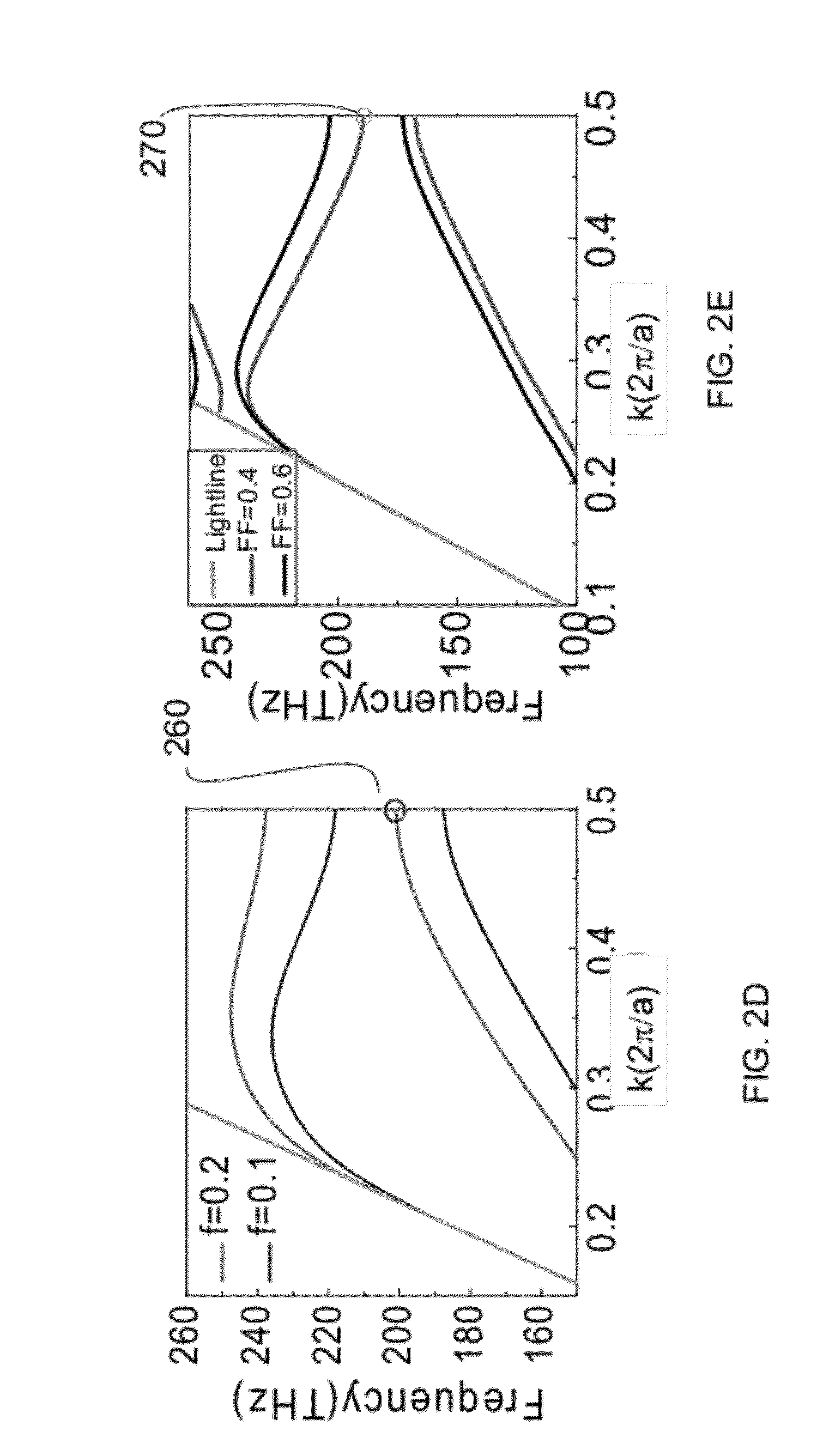
[0036]The design approach of the present invention is deterministic in the sense that it does not involve any trial-based manipulation of the cavity geometry, including hole shifting, re-sizing and overall cavity re-scaling. The present approach results in ultra-high Q cavity by-design. Moreover, the final cavity has resonance that is typically less than 1% away from a desired operation frequency. Therefore, the method of the present invention allows for fast design of optical cavities with predetermined resonant frequency and by-design ultra-high Q. Further, the design and manufacturing method of the present invention requires only computationally inexpensive, photonic band calculations (e.g. using a plane wave expansion method). Ultra-high Q cavity devices can be manufactured according to the design parameters using electron beam or optical lithography methods.

[0037]The design method is based on the realization of a Gaussian-like field profile proposed in Q. Quan, P. B. Deotare, a...


PUM


Abstract

A deterministic design and manufacturing of an ultrahigh Q-factor, wavelength-scale optical cavity is invented and experimentally demonstrated. The design can be implemented on photonic crystal nanobeam cavities, which are based on 1D optical waveguides. The waveguide has dielectric index alternations that provide constructive interference and produces optical resonance.

Description

CROSS-REFERENCE TO RELATED APPLICATIONS[0001]The present application claims the benefit of the filing date of U.S. Provisional Patent Application Ser. No. 61 / 387,634 filed by the present inventors on Sep. 29, 2010.[0002]The aforementioned provisional patent application is hereby incorporated by reference in its entirety.STATEMENT REGARDING FEDERALLY SPONSORED RESEARCH OR DEVELOPMENT[0003]Not applicable.BACKGROUND OF THE INVENTION[0004]1. Field Of The Invention[0005]The present invention relates to photonic crystal (PhC) cavities and more particularly to a novel method for deterministically designing and making a high quality factor, wavelength scale photonic crystal nanobeam cavity. The deterministic method of the present invention can be applied to different material systems and to cavities resonant at different ranges of wavelengths as well.[0006]2. Brief Description Of The Related Art[0007]Photonic crystal (PhC) cavities with high quality (Q) factors and wavelength-sc...

Claims


Application Information

Patent Timeline
Patent Type & Authority Applications(United States)
IPC IPC(8): G02B6/32B44C1/22G02B6/34
CPCG02B6/1225B82Y20/00G02B6/30G02B6/29356
Inventor QUAN, QIMINLONCAR, MARKO
Owner PRESIDENT & FELLOWS OF HARVARD COLLEGE
Learn More