Multi-layer variable micro structure for sensing substance
a micro structure and multi-layer technology, applied in solid-state devices, instruments, material analysis, etc., can solve the problem of weak raman scattering signal of conventional raman spectroscopy for trace chemical detection, and achieve the effect of enhancing the intensity of scattered ligh
- Summary
- Abstract
- Description
- Claims
- Application Information
AI Technical Summary
Benefits of technology
Problems solved by technology
Method used
Image
Examples
Embodiment Construction
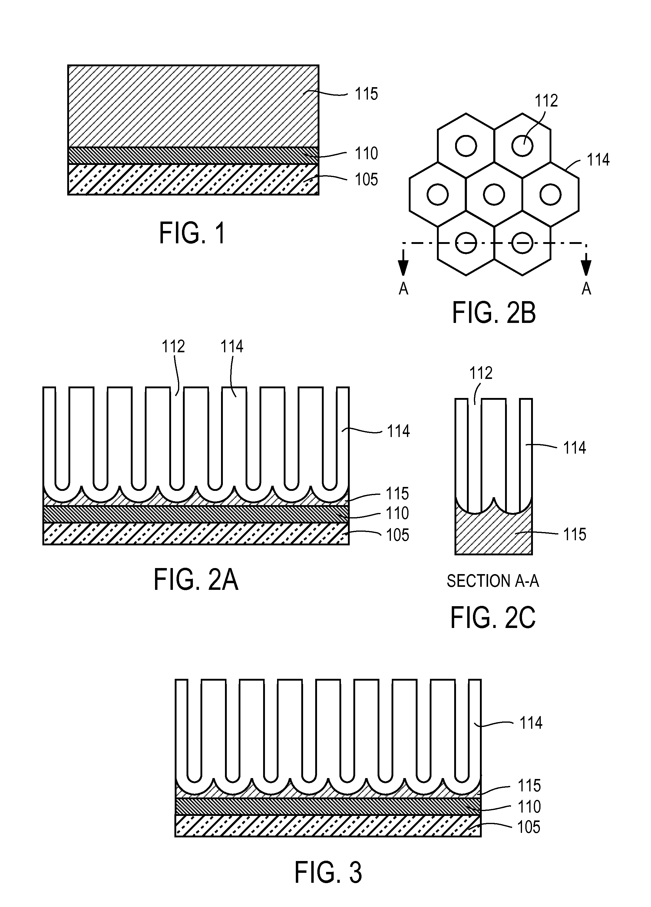
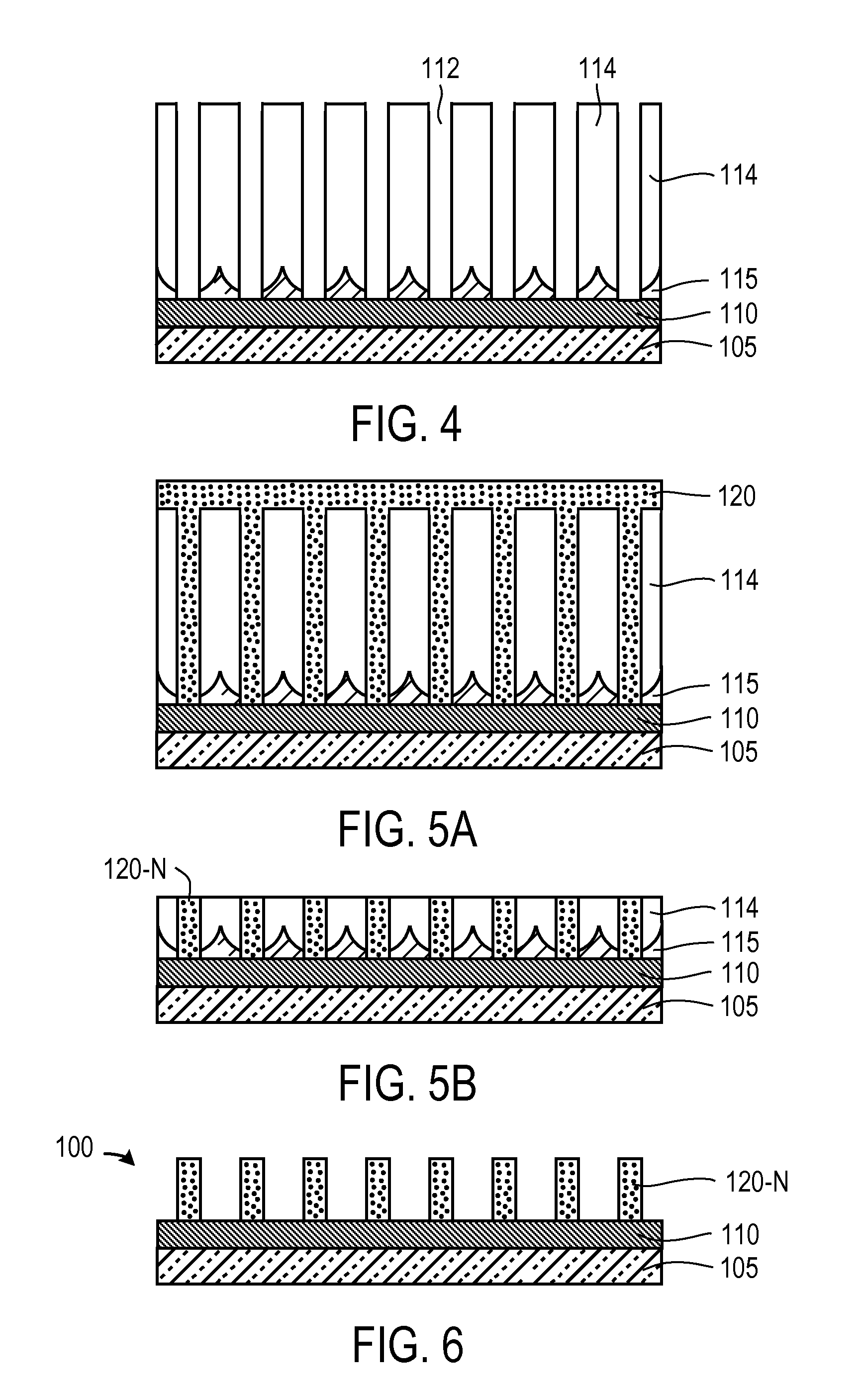
[0067]Referring to FIGS. 1 to 6 for a series of processing steps to fabricate a nano-structured noble metal surface of this application, FIG. 1 shows a two-layer structure with n-type (100) silicon wafer (3-8 Ω-cm) or oxidized (30-50 nm SiO2) p-type (100) silicon wafers (5-10 mΩ-cm), an electrically and thermally conductive layer 110 deposited on a (100) silicon substrate 105. The thickness of the conductive layer 110, such as Ti and Ni, is optimized to provide i) best adhesion to a subsequently deposited noble metal film, such as Ag, or Au film, etc., ii) electrical conductive film to apply electrical bias to sensing surface in field application, iii) thermal conductive layer to apply lower temperature of sensing surface, iv) thermal heat sink film to conduct localized heat generated by excitation of a light source. The thickness of this metal film is usually controlled in the range of 50 Å-50,000 Å, or 100 Å-1,000 Å. Then an aluminum layer 115 with purity of 99.999% and thickness ...
PUM
 Abstract
Description
Claims
Application Information
 - R&D
- Intellectual Property
- Life Sciences
- Materials
- Tech Scout
- Unparalleled Data Quality
- Higher Quality Content
- 60% Fewer Hallucinations
Browse by: Latest US Patents, China's latest patents, Technical Efficacy Thesaurus, Application Domain, Technology Topic, Popular Technical Reports.
© 2025 PatSnap. All rights reserved.Legal|Privacy policy|Modern Slavery Act Transparency Statement|Sitemap|About US| Contact US: help@patsnap.com


