Organic light-emitting display panel, display device, and method of manufacturing organic light-emitting display panel
- Summary
- Abstract
- Description
- Claims
- Application Information
AI Technical Summary
Benefits of technology
Problems solved by technology
Method used
Image
Examples
embodiment 1
Structure of Display Panel 100
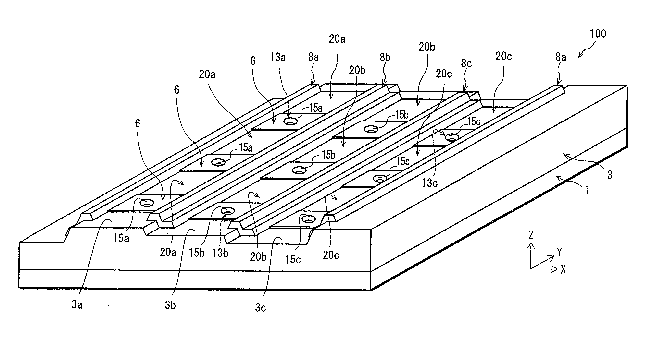
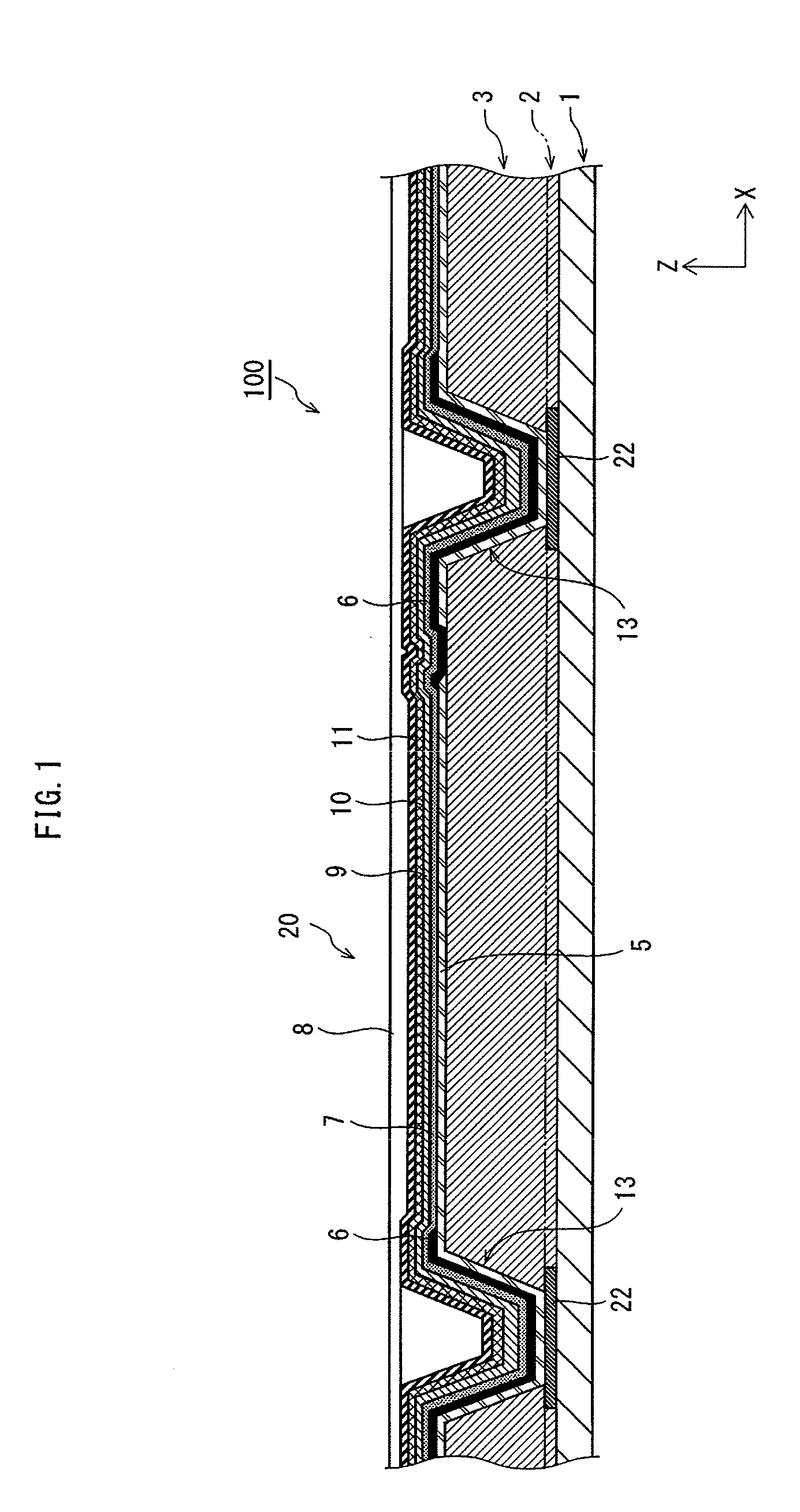
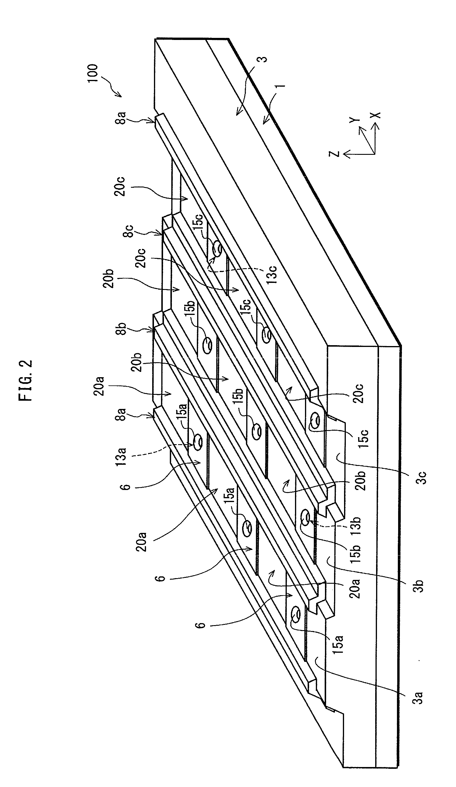
[0145]FIG. 1 is a cross-section diagram schematically showing the structure of the main parts of a display panel 100 according to Embodiment 1. FIG. 2 is a perspective view showing the structure of the main parts of the display panel 100.
[0146]The display panel unit 100 is an organic light-emitting display panel that uses the phenomenon of electroluminescence occurring in organic material. Pixels are arranged in a matrix in the lateral and longitudinal (X and Y) directions in the display panel 100. Each pixel is formed by three adjacent sub-pixels whose colors are respectively red, green, and blue (RGB). The organic light-emitting elements 20a, 20b, and 20c shown in FIG. 2 are top-emission type light-emitting elements. The organic light-emitting elements 20a are sub-pixels of a first color (blue), the organic light-emitting elements 20b are sub-pixels of a second color (green), and organic light-emitting elements 20c are sub-pixels of a third color (red...
embodiment 2
[0313]In Embodiment 1, the depth of the contact holes 13 is changed by forming levels in the interlayer insulation film 3. Alternatively, the upper surface of the interlayer insulation film may be planarized, and the height of the upper surface of the substrate where the contact hole corresponding to each color is to be formed may be changed in order to change the film thickness of the interlayer insulation film and to change the depth of the contact holes.
[0314]FIG. 11 is a cross-section diagram schematically showing a display panel 80 according to the present Embodiment. FIG. 11 shows a cross-section corresponding to the cross section A-A′ of FIG. 3A. Note that the light-emitting layer, cathode layer, etc. are omitted from FIG. 11.
[0315]In the present Embodiment, the structure shown in FIGS. 3A and 3C of Embodiment 1 is basically adopted. However, the cross-sectional shape of the substrate and of the interlayer insulation film differs. Note that the same reference numbers are used...
PUM
 Abstract
Description
Claims
Application Information
 - R&D
- Intellectual Property
- Life Sciences
- Materials
- Tech Scout
- Unparalleled Data Quality
- Higher Quality Content
- 60% Fewer Hallucinations
Browse by: Latest US Patents, China's latest patents, Technical Efficacy Thesaurus, Application Domain, Technology Topic, Popular Technical Reports.
© 2025 PatSnap. All rights reserved.Legal|Privacy policy|Modern Slavery Act Transparency Statement|Sitemap|About US| Contact US: help@patsnap.com


