Photoelectric conversion element, manufacturing method thereof, optical sensor, and solar cell
a technology of photoelectric conversion and manufacturing method, which is applied in the manufacture of final products, sustainable manufacturing/processing, electrolytic capacitors, etc., can solve the problems of high power generation cost and become a barrier to their spread, and achieve excellent usefulness and photoelectric conversion
- Summary
- Abstract
- Description
- Claims
- Application Information
AI Technical Summary
Benefits of technology
Problems solved by technology
Method used
Image

Examples
first embodiment
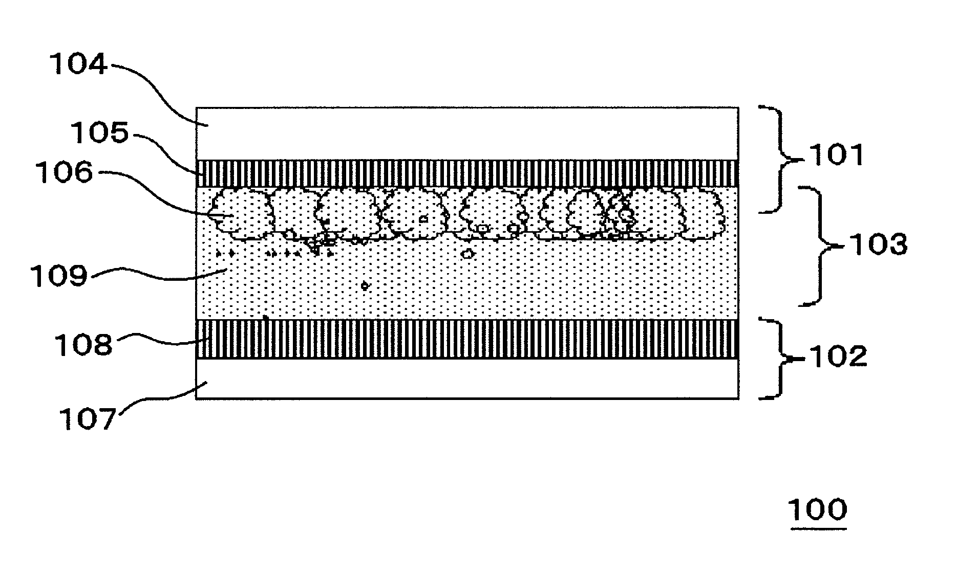
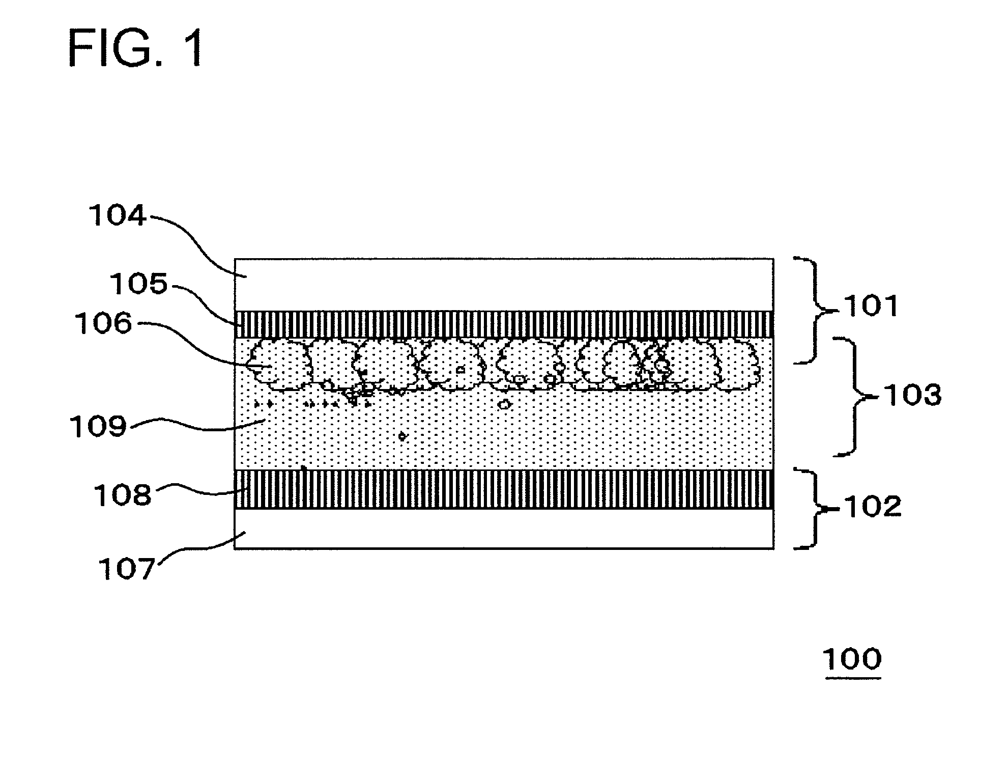
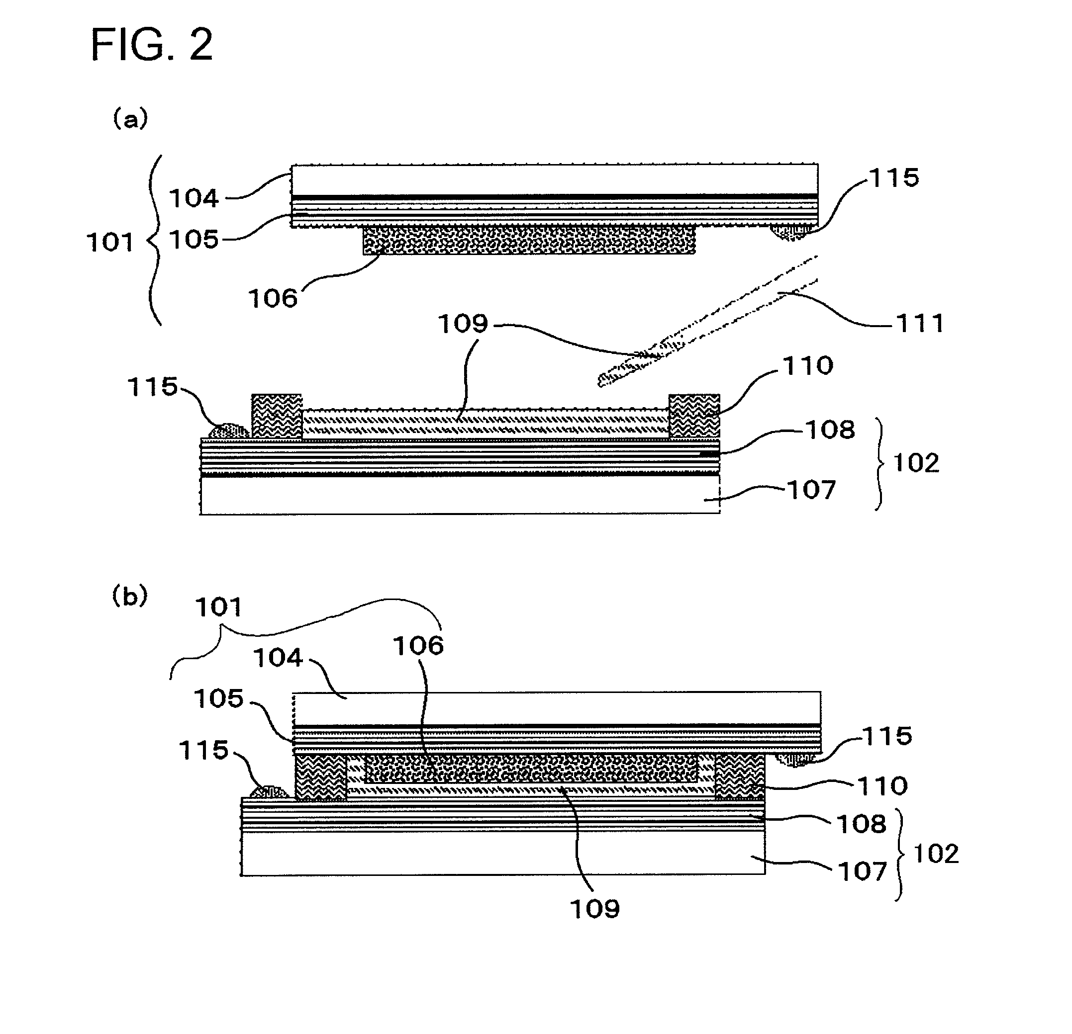
[0030]FIG. 1 is a sectional view illustrating the configuration of a photoelectric conversion element according to an embodiment of the invention. A photoelectric conversion element 100 shown in FIG. 1 includes a photoelectrode 101 including a semiconductor layer (a porous semiconductor layer 106) and a transparent conductive substrate (a transparent electrode 104) and a counter electrode (a transparent electrode 107) disposed to face the photoelectrode 101. The photoelectrode 101 is formed of a substrate (a transparent conductive substrate, a transparent electrode 104) having the porous semiconductor layer 106. The transparent electrode 107 is stacked to face the photoelectrode 101.
[0031]A nitroxyl radical compound having a structure of 4,4,5,5-tetraalkyl imidazoline-1-oxyl 3-oxide expressed by General Formula 1 as a compound having a light-absorbing function and a redox function is mainly included between the photoelectrode 101 and the transparent electrode 107. Here, the term “be...
second embodiment
[0080]The photoelectric conversion element 100 (FIG. 1) according to the first embodiment is very suitably used, for example, as a dye-sensitized solar cell.
[0081]When solar light is applied from the side of the photoelectrode 101 of the photoelectric conversion element 100, the solar light passes through the transparent electrode 104 and the conductive layer 105 in this order and is applied to the dye (not shown in the drawing) adsorbed to the porous semiconductor layer 106. The dye absorbs the light and is thus excited. Electrons generated by this excitation migrate to the conductive layer 105 from the porous semiconductor layer 106. The electrons migrating to the conductive layer 105 migrates to the counter electrode 102 via an external circuit and returns to the dye via the organic compound solution 109 from the conductive layer 108. In this way, current flows to constitute a solar cell.
[0082]Plural photoelectric conversion elements according to the invention can be used as a ph...
example 1
[0100]A photoelectric conversion element according to the invention was manufactured as follows. First, 5 g of a commercially-available titanium dioxide powder (product name: P25, made by Nippon Aerosil Co., Ltd.), 20 mL of 15 vol % solution of acetate, 0.1 mL of surfactant (product name: Triton X-100, made by Sigma-Aldrich Co., Ltd.), and 0.3 g of polyethylene glycol (with a molecular weight of 20,000) were stirred with a stirring mixer to prepare a titanium dioxide paste for forming a porous semiconductor layer.
[0101]Then, the titanium dioxide paste was applied by an appropriate amount (application area: 3 cm×3 cm) onto an ITO glass substrate (6 cm×4 cm, sheet resistance: 20Ω / □) so as to have a thickness of 20 μm by the use of a doctor blade method. Here, the part to which the paste was not applied was used as the electrode extraction portion and the sealing portion. Four through-holes with 0.5 mm□ were formed between the applied portion and the sealing portion. The electrode was ...
PUM
 Abstract
- (where A in General Formula 1 represents a substituted or unsubstituted aromatic group and may contain one or more atoms of oxygen, nitrogen, sulfur, silicon, phosphorus, boron, or halogen and the aromatic group may be obtained by condensing a plurality of aromatic groups).
Description
Claims
Application Information
 - R&D
- Intellectual Property
- Life Sciences
- Materials
- Tech Scout
- Unparalleled Data Quality
- Higher Quality Content
- 60% Fewer Hallucinations
Browse by: Latest US Patents, China's latest patents, Technical Efficacy Thesaurus, Application Domain, Technology Topic, Popular Technical Reports.
© 2025 PatSnap. All rights reserved.Legal|Privacy policy|Modern Slavery Act Transparency Statement|Sitemap|About US| Contact US: help@patsnap.com