Manufacturing method of liquid crystal display device
a liquid crystal display and manufacturing method technology, applied in non-linear optics, instruments, optics, etc., can solve the problems of uneven rubbing and uneven rubbing, and achieve the effect of reducing and eliminating the influence of rubbing shadows
- Summary
- Abstract
- Description
- Claims
- Application Information
AI Technical Summary
Benefits of technology
Problems solved by technology
Method used
Image

Examples
first embodiment
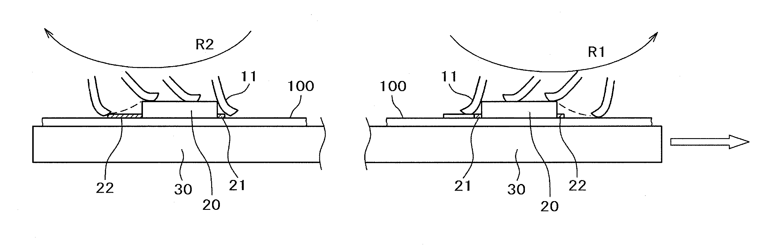
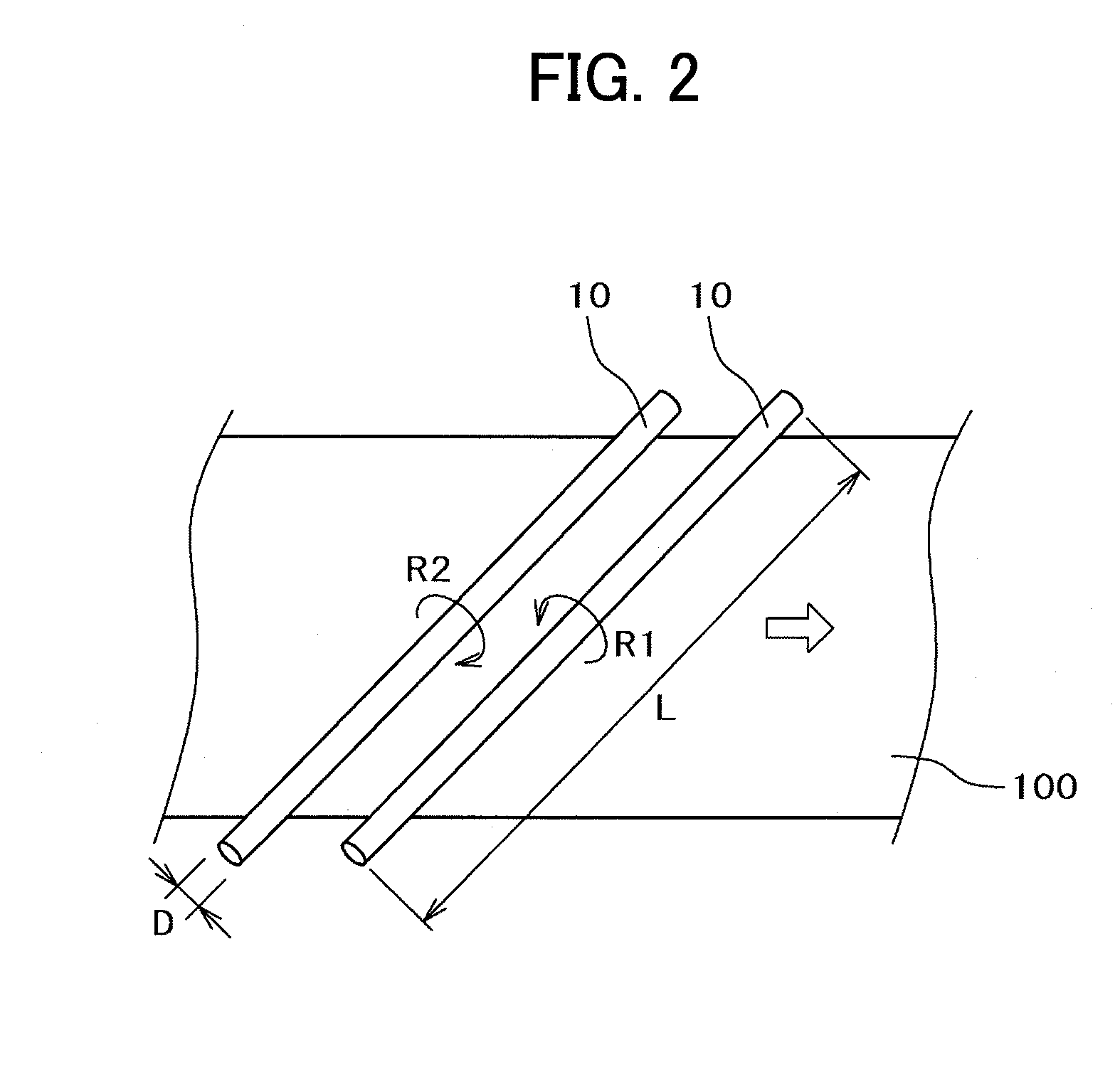
[0032]FIG. 1 is a schematic drawing showing a rubbing step according to an embodiment of the present invention. In FIG. 1, a TFT substrate 100 is placed on a rubbing stage 30. The TFT substrate 100 has asperities represented by TFT wiring 20. The TFT wiring 20 represents asperities and does not indicate a specific wire. In FIG. 1, an alignment layer 109 is omitted. The rubbing stage 30 having the TFT substrate 100 moves at, e.g., 30 mm / sec in the direction of a white arrow.
[0033]In FIG. 1, two rubbing rollers 10 are disposed to rub the TFT substrate 100. The two rubbing rollers 10 rotate in opposite directions. The two rubbing rollers 10 rotate at, e.g., 1500 rpm. The TFT substrate 100 is first rubbed by the left rubbing roller 10 and then rubbed by the right rubbing roller 10.
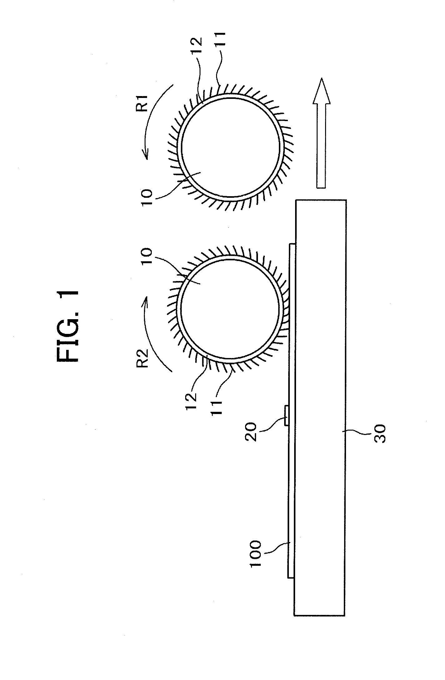
[0034]FIG. 2 is a perspective view showing a state of rubbing on the TFT substrate 100. In FIG. 2, the two rubbing rollers 10 are inclined with respect to the TFT substrate 100 in plan view. Thus the initial o...
PUM
 Abstract
Description
Claims
Application Information
 - R&D
- Intellectual Property
- Life Sciences
- Materials
- Tech Scout
- Unparalleled Data Quality
- Higher Quality Content
- 60% Fewer Hallucinations
Browse by: Latest US Patents, China's latest patents, Technical Efficacy Thesaurus, Application Domain, Technology Topic, Popular Technical Reports.
© 2025 PatSnap. All rights reserved.Legal|Privacy policy|Modern Slavery Act Transparency Statement|Sitemap|About US| Contact US: help@patsnap.com