Liquid crystal display device
a liquid crystal display and display device technology, applied in the direction of digital storage, instruments, computing, etc., can solve the problem of high driving voltage, and achieve the effect of reducing the amplitude voltage of an image signal written into a signal lin
- Summary
- Abstract
- Description
- Claims
- Application Information
AI Technical Summary
Benefits of technology
Problems solved by technology
Method used
Image
Examples
embodiment 1
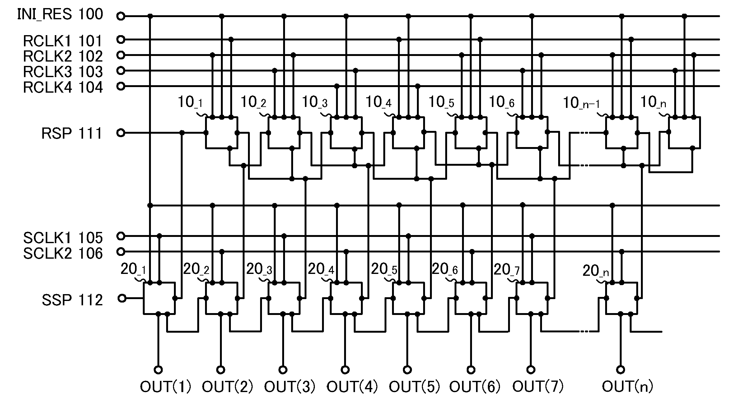
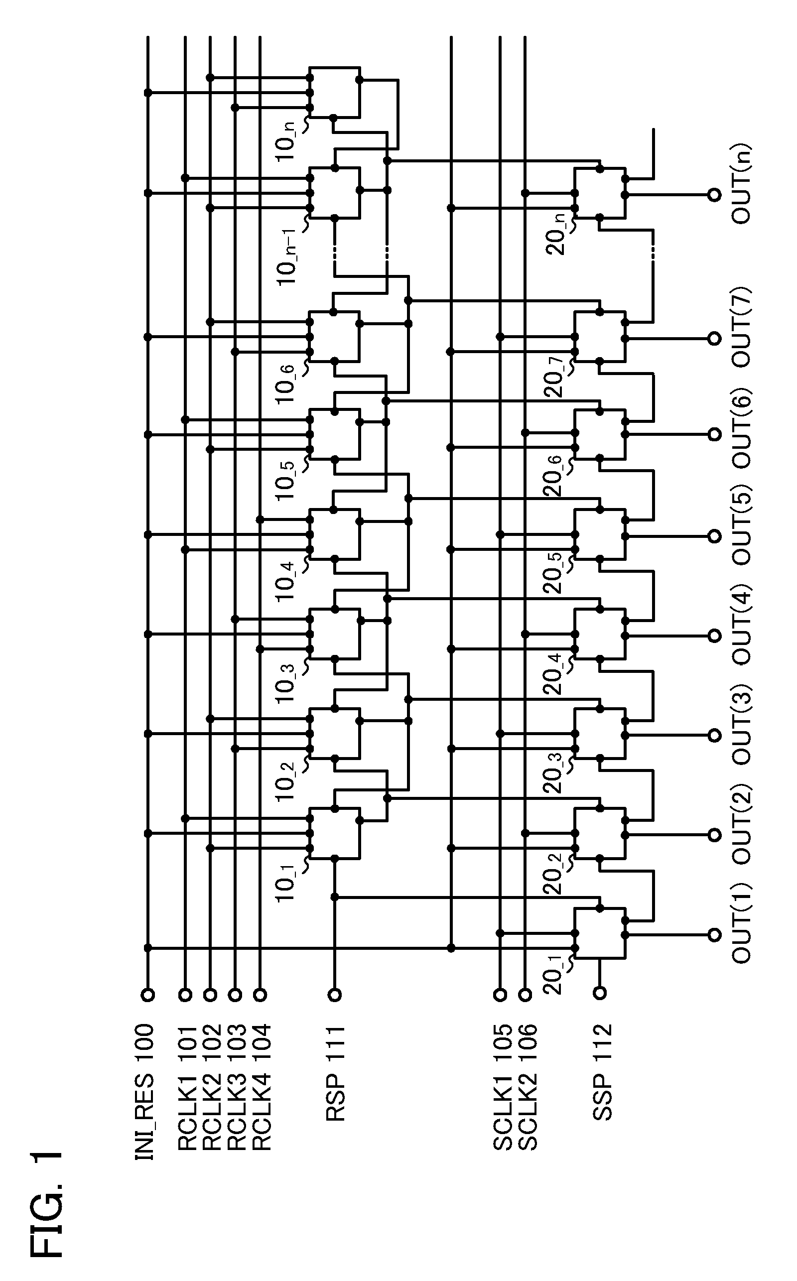
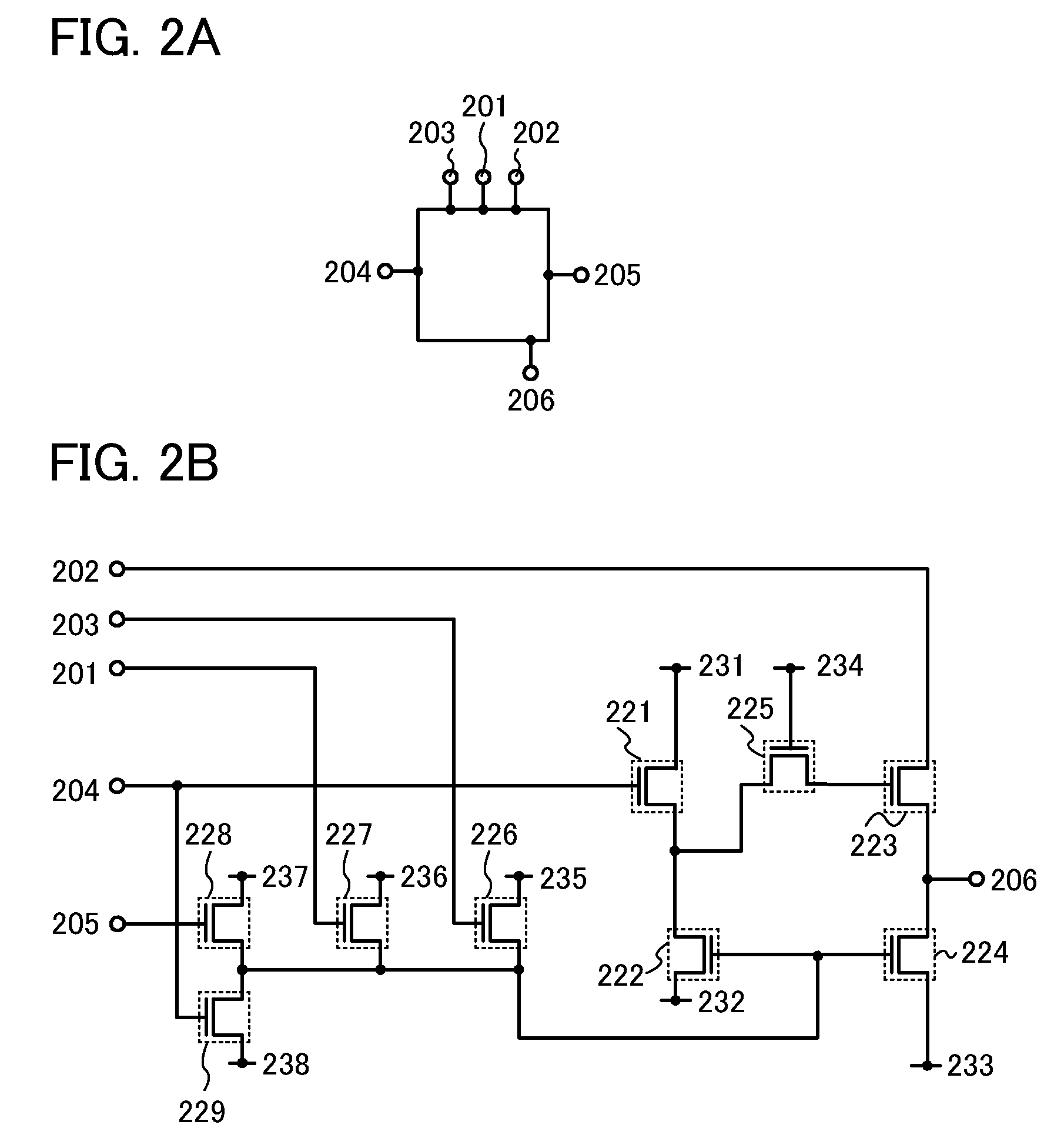
In this embodiment, as for a shift register which is provided in a common line driver circuit, examples of a reset pulse output circuit, a set pulse output circuit, and a shift register including the reset pulse output circuit and the set pulse output circuit will be described with reference to FIG. 1, FIGS. 2A and 2B, FIGS. 3A and 3B, FIG. 4, FIGS. 5A and 5B, FIGS. 6A and 6B, FIGS. 7A and 7B, FIGS. 8A and 8B, FIGS. 9A and 9B, FIGS. 10A and 10B, and FIG. 22.
First, the structure of a liquid crystal display device including a common line driver circuit provided with a shift register, which is described in this embodiment, will be described with reference to FIG. 22.
As illustrated in FIG. 22, the liquid crystal display device includes, over a substrate 2207, a pixel portion 2202 in which a plurality of pixels 2201 are arranged (arrayed) in matrix in a row direction and a column direction, and a signal line driver circuit 2203, a scan line driver circuit 2204, and a common line driver c...
embodiment 2
In this embodiment, the configuration of a shift register provided in a common line driver circuit, which is different from that in Embodiment 1, will be described.
The configuration of the shift register in this embodiment will be described with reference to FIG. 11. The shift register includes a first reset pulse output circuit 30—1 to an n-th reset pulse output circuit 30, (n is a natural number of greater than or equal to 2), and a first set pulse output circuit 20—1 to an n-th set pulse output circuit 20n.
The reset pulse output circuit will be described with reference to FIGS. 12A and 12B.
In Embodiment 1, as shown in FIG. 1, each of the fifth input terminals 205 of the first reset pulse output circuit 10—1 to an (n−1)-th reset pulse output circuit 10—1 (n is a natural number of greater than or equal to 2) is connected to the first output terminal 206 of the reset pulse output circuit in the subsequent stage. In this embodiment, as shown in FIG. 11, each of the first reset pulse ...
embodiment 3
In this embodiment, the configuration of a shift register provided in a common line driver circuit, which is different from those in Embodiments 1 and 2, will be described with reference to FIG. 13, FIG. 14, and FIG. 15. In this embodiment, an example in which a first shift register and a second shift register are provided in the common line driver circuit will be described.
First, the configuration of the first shift register including a first reset pulse output circuit and a first set pulse output circuit will be described below.
The configuration of the first shift register in this embodiment will be described with reference to FIG. 13. The first shift register includes a first reset pulse output circuit 40—1 to an (2m−1)-th reset pulse output circuit 40—2m−1 (m is a natural number of greater than or equal to 2), and a first set pulse output circuit 50—1 to an (2m−1)-th set pulse output circuit 50—2m−1 (m is a natural number of greater than or equal to 2).
In the reset pulse output ...
PUM
 Abstract
Description
Claims
Application Information
 - R&D
- Intellectual Property
- Life Sciences
- Materials
- Tech Scout
- Unparalleled Data Quality
- Higher Quality Content
- 60% Fewer Hallucinations
Browse by: Latest US Patents, China's latest patents, Technical Efficacy Thesaurus, Application Domain, Technology Topic, Popular Technical Reports.
© 2025 PatSnap. All rights reserved.Legal|Privacy policy|Modern Slavery Act Transparency Statement|Sitemap|About US| Contact US: help@patsnap.com


