Method of fabricating semiconductor device

a semiconductor and device technology, applied in the field of integrated circuits, can solve the problems of difficult chip reduction, small saturated current of medium voltage devices, poor performance of the same, etc., and achieve the effects of improving performance, reducing the dimension of products, and increasing saturated curren

Active Publication Date: 2011-10-06
UNITED MICROELECTRONICS CORP
View PDF2 Cites 2 Cited by
  • Summary
  • Abstract
  • Description
  • Claims
  • Application Information

AI Technical Summary

Benefits of technology

[0006]The present invention further provides a method of fabricating a semiconductor device. The method is simple and low-cost and meets the market requirement. A semiconductor device manufactured by the method includes a high voltage device, a medium voltage device and a low voltage device formed on a single chip. The medium voltage device has a higher saturated current, so that the semiconductor device has a better performance when applied to the voltage level shift circuit of a gate driver. The dimension of the medium voltage device is smaller than that of the high voltage device, so that the whole dimension of the product can be significantly reduced.
[0027]In the present invention, the medium voltage device of the semiconductor device has a higher saturated current, so that the semiconductor device has a better performance when applied to the voltage level shift circuit of a gate driver. Further, the dimension of the medium voltage device is smaller than that of the high voltage device, so that the whole dimension of the product can be significantly reduced. In addition, the method of fabricating a semiconductor device is simple and low-cost and meets the market requirement.

Problems solved by technology

However, during the operation, the saturated current of the medium voltage device is small and the performance of the same is bad.
Further, the occupied chip area becomes greater due to the larger size of the high voltage device and the medium voltage device, so that the chip reduction becomes difficult and a higher chip cost is caused.

Method used


Image

  • Method of fabricating semiconductor device
  • Method of fabricating semiconductor device
  • Method of fabricating semiconductor device

Examples


Embodiment Construction

[0034]The present invention will now be described more specifically with reference to the following embodiments. It is to be noted that the following descriptions of preferred embodiments of this invention are presented herein for purpose of illustration and description only. It is not intended to be exhaustive or to be limited to the precise form disclosed.

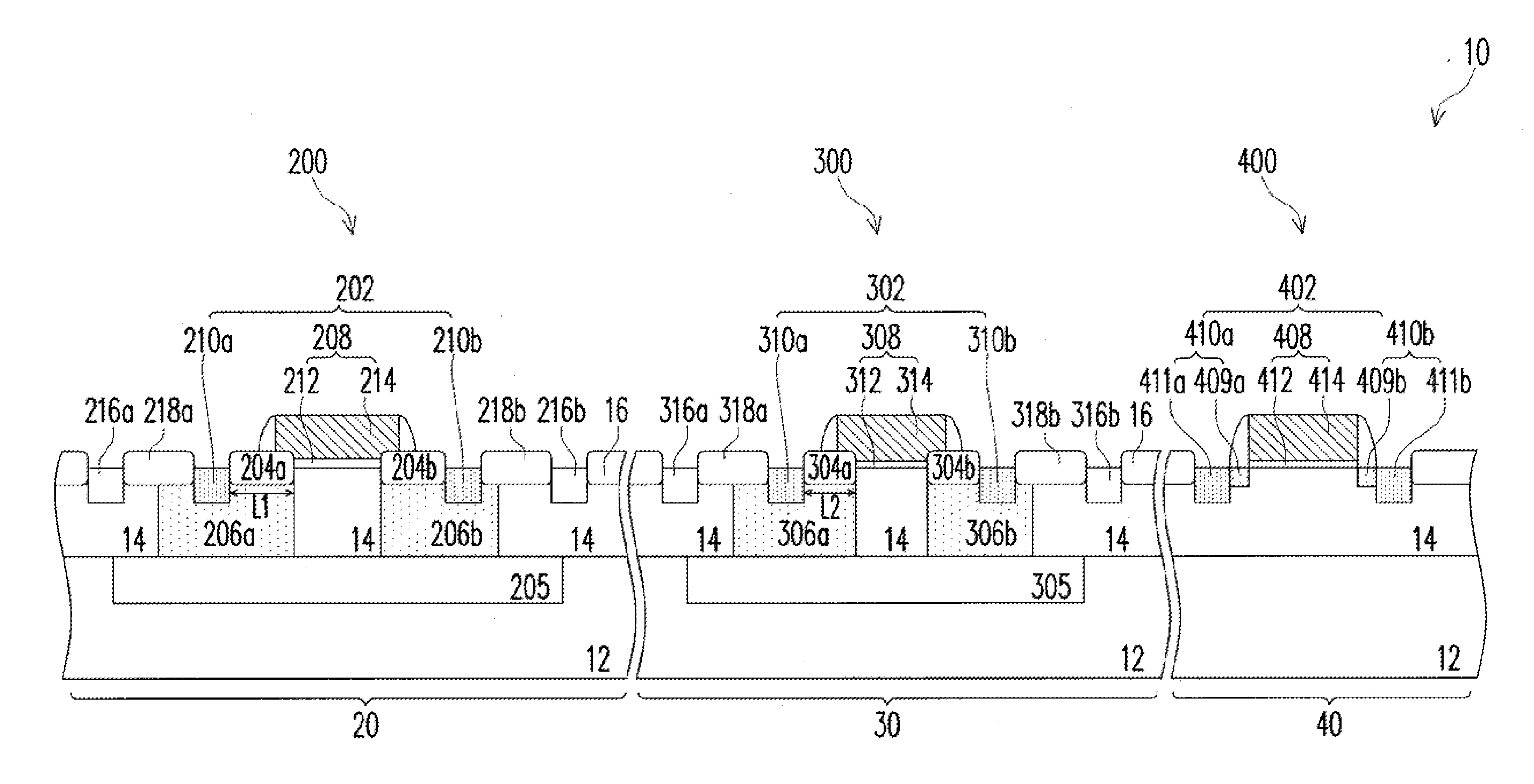
[0035]FIG. 1 schematically illustrates a cross-section view of a semiconductor device according to an embodiment of the present invention.

[0036]Referring to FIG. 1, a semiconductor device 10 of the present invention includes a substrate 12 of a first conductivity type or a substrate 12 having a first well 14 of a first conductivity type therein, a high voltage device 200 of a second conductivity type, a medium voltage device 300 of the second conductivity type and a low voltage device 400 of the second conductivity type. In the following embodiments, the present invention is illustrated by a substrate 12 having a first well 14 of...


PUM


Abstract

A method of fabricating a semiconductor device utilizes a substrate including a high voltage circuit area, a medium voltage circuit area and a low voltage circuit area. A first well of a first conductivity type is formed. Two separate second wells of a second conductivity type are formed in the first well and two separate isolation structures are formed respectively in the second wells in each of the high voltage circuit area and the medium voltage circuit area. A first gate dielectric layer is formed in the high voltage circuit area. A second gate dielectric layer that is thinner than the first gate dielectric layer is formed in each of the medium voltage circuit area and the low voltage circuit area. A gate is formed. Two source and drain regions of the second conductivity type are respectively formed. The method is simple and low-cost and meets the market requirement.

Description

CROSS-REFERENCE TO RELATED APPLICATION[0001]This is a divisional application of an application Ser. No. 12 / 253,822, filed Oct. 17, 2008. The entirety of the above-mentioned patent are hereby incorporated by reference herein and made a part of this specification.FIELD OF THE INVENTION[0002]The present invention relates to an integrated circuit and a method of fabricating the same, and more generally to a semiconductor device and a method of fabricating the same.BACKGROUND OF THE INVENTION[0003]Multi-function products with light weights, slim shapes and small sizes have become the mainstream in the market as the technology is developed. Accordingly, the operation voltage of the internal circuit of a single technology product is reduced, and the number and types of circuits or integrated circuit chips are required more.[0004]Generally, the voltage level shift among integrated circuits with different voltage levels is performed through a voltage level shift circuit. A typical voltage le...

Claims


Application Information

Patent Timeline
Patent Type & Authority Applications(United States)
IPC IPC(8): H01L21/8234
CPCH01L21/823814H01L21/823878H01L21/823857
Inventor CHEN, CHIN-LUNGHUANG, HAN-MIN
Owner UNITED MICROELECTRONICS CORP
Why Eureka
Try Eureka