Orientation film, orientation film material, liquid crystal display having orientation film, and method for forming the same
a technology of orientation film and alignment film, which is applied in the direction of instruments, synthetic resin layered products, transportation and packaging, etc., can solve the problems of difficulty in realizing high luminance and the insufficient characteristics of alignment film made of one polymer, and achieve the effect of suppressing the image sticking caused by changes in the pretilt angl
- Summary
- Abstract
- Description
- Claims
- Application Information
AI Technical Summary
Benefits of technology
Problems solved by technology
Method used
Image
Examples
example 1
Example 1-1
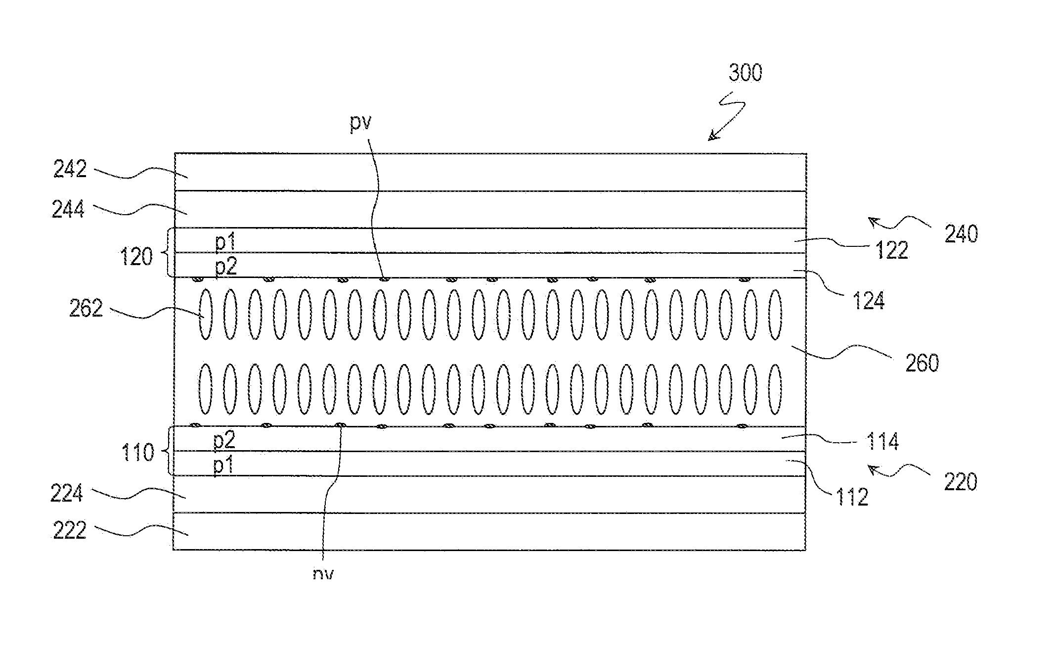
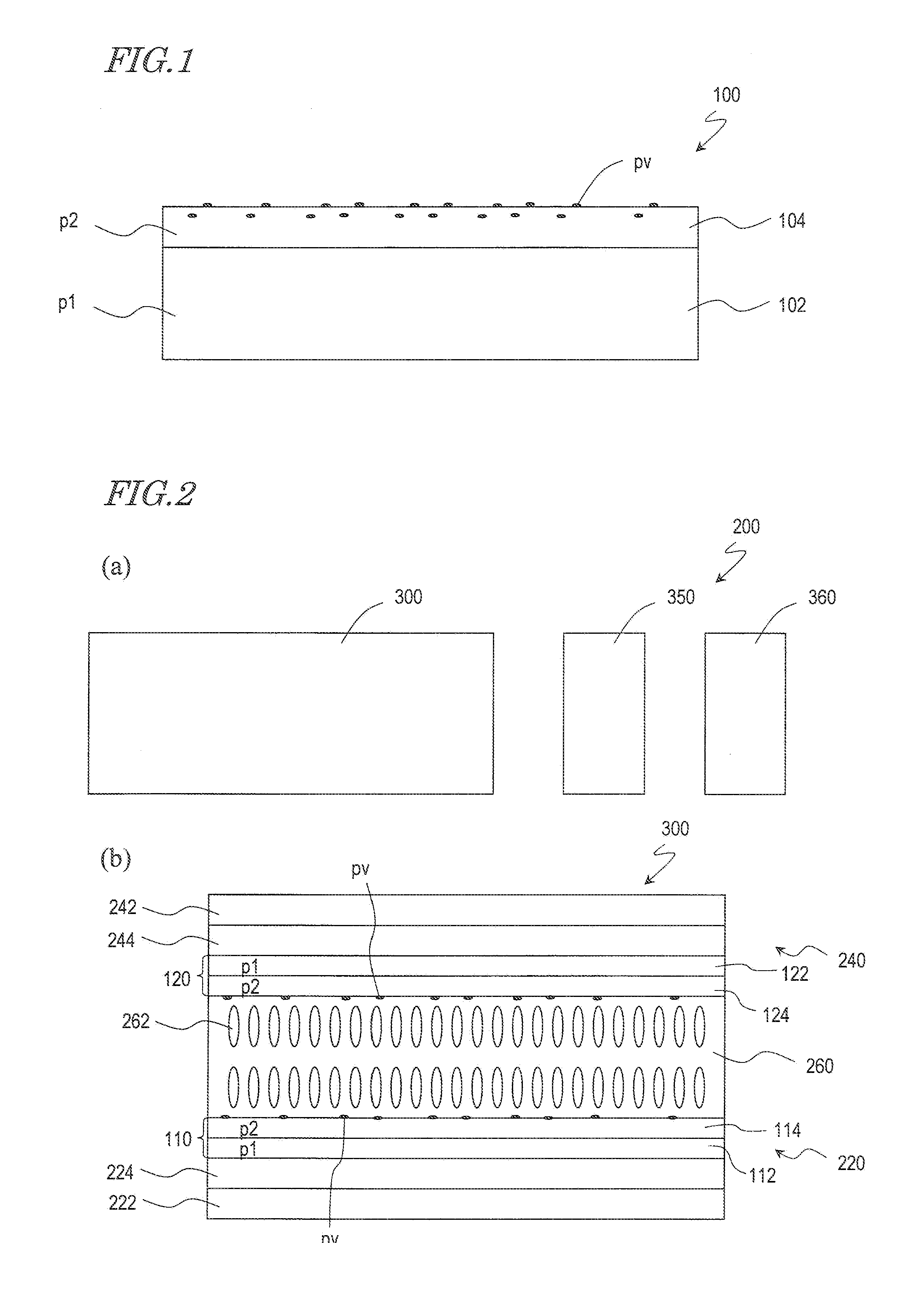
[0174]Hereinafter, with reference to FIG. 2 and FIG. 6, an alignment film and a liquid crystal display device of Example 1-1 will be described. The liquid crystal display device of Example 1-1 also operates in the RTN mode.
[0175]First, on a principal face of the first insulative substrate 222, although not shown in the figures, TFTs and wiring lines connected to the TFTs, and an insulating layer and the like were formed, upon which the pixel electrodes 224 were formed. Similarly, on a principal face of the second insulative substrate 242, although not shown in the figures, a colored layer having color filters, and an insulating layer and the like were formed, upon which the counter electrode 244 was formed.
[0176]Next, a vertical-alignment type alignment film material was provided. This alignment film material was an alignment film material intended for use in a photo-alignment film. The alignment film material was formed by, after allowing a precursor of the first polyimi...
example 1-2
[0186]Hereinafter, with reference to FIG. 2 and FIG. 6, an alignment film and a liquid crystal display device of Example 1-2 will be described. The liquid crystal display device of Example 1-2 also operates in the RTN mode.
[0187]First, on a principal face of the first insulative substrate 222, although not shown in the figures, TFTs and wiring lines connected to the TFTs, and an insulating layer and the like were formed, upon which the pixel electrodes 224 were formed. Similarly, on a principal face of the second insulative substrate 242, although not shown in the figures, a colored layer having color filters, and an insulating layer and the like were formed, upon which the counter electrode 244 was formed.
[0188]Next, a vertical-alignment type alignment film material was provided. This alignment film material was an alignment film material intended for use in a photo-alignment film. The alignment film material was formed by, after allowing a precursor of the first polyimide p1 and t...
example 1-3
[0196]Hereinafter, with reference to FIG. 2 and FIG. 6, an alignment film and a liquid crystal display device of Example 1-3 will be described. The liquid crystal display device of Example 1-3 also operates in the RTN mode.
[0197]First, on a principal face of the first insulative substrate 222, although not shown in the figures, TFTs and wiring lines connected to the TFTs, and an insulating layer and the like were formed, upon which the pixel electrodes 224 were formed. Similarly, on a principal face of the second insulative substrate 242, although not shown in the figures, a colored layer having color filters, and an insulating layer and the like were formed, upon which the counter electrode 244 was formed.
[0198]Next, a vertical-alignment type alignment film material was provided. This alignment film material was an alignment film material intended for use in a photo-alignment film. The alignment film material was formed by, after allowing a precursor of the first polyimide p1 and t...
PUM
| Property | Measurement | Unit |
|---|---|---|
| Fraction | aaaaa | aaaaa |
| Fraction | aaaaa | aaaaa |
| Fraction | aaaaa | aaaaa |
Abstract
Description
Claims
Application Information
 - R&D
- Intellectual Property
- Life Sciences
- Materials
- Tech Scout
- Unparalleled Data Quality
- Higher Quality Content
- 60% Fewer Hallucinations
Browse by: Latest US Patents, China's latest patents, Technical Efficacy Thesaurus, Application Domain, Technology Topic, Popular Technical Reports.
© 2025 PatSnap. All rights reserved.Legal|Privacy policy|Modern Slavery Act Transparency Statement|Sitemap|About US| Contact US: help@patsnap.com


