Optical component, method of manufacturing optical component, and electronic apparatus
a technology of optical components and optical components, applied in the field of optical components, can solve problems such as adverse effects on products, and achieve the effect of high dust-proof performance and high accuracy
- Summary
- Abstract
- Description
- Claims
- Application Information
AI Technical Summary
Benefits of technology
Problems solved by technology
Method used
Image
Examples
application example 2
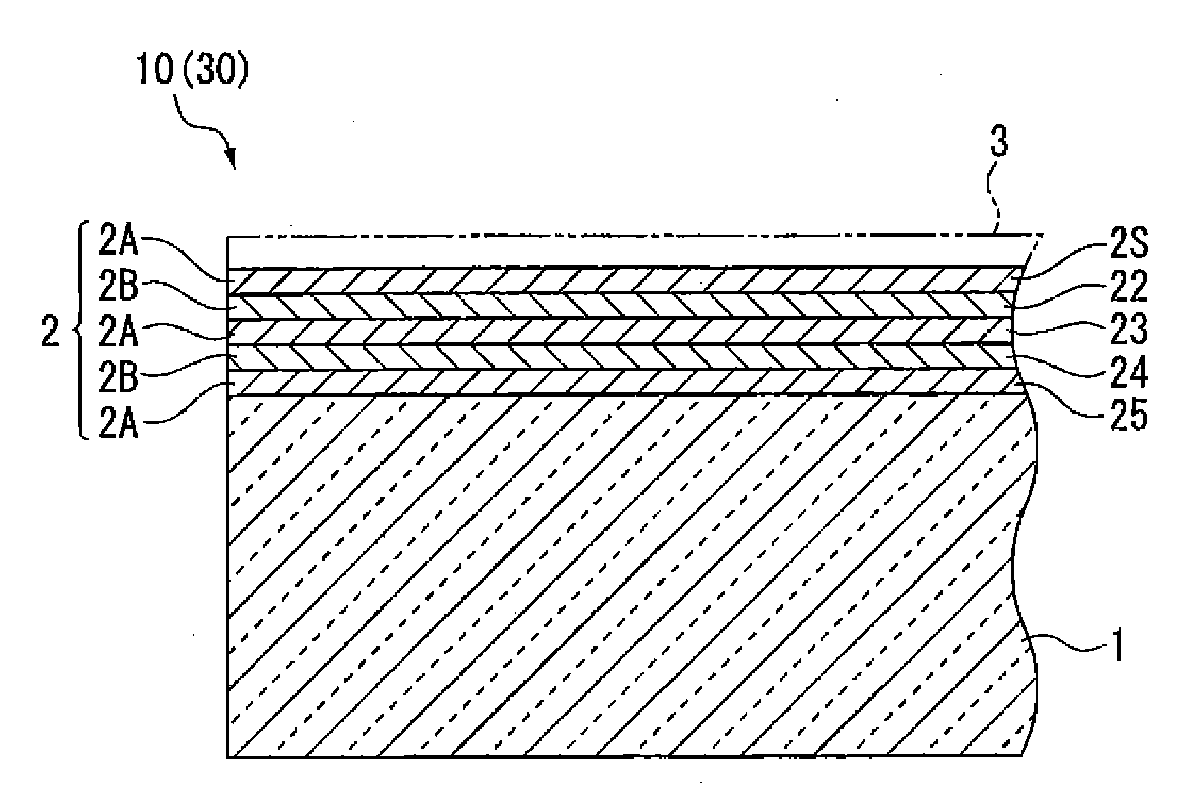
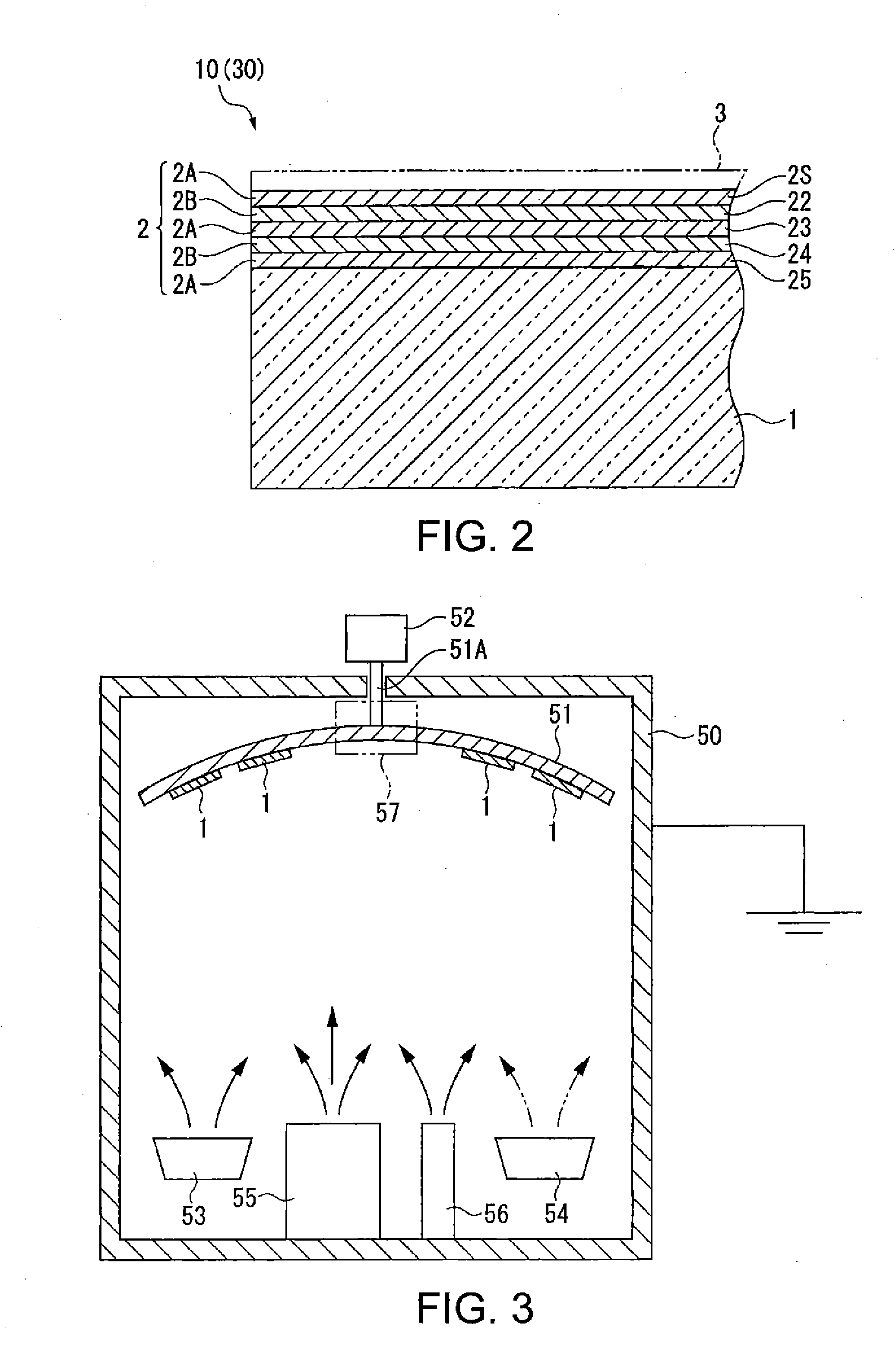
In the optical component according to the above application example of the invention, the layer of metal oxide near the outermost layer may include a layer of zirconium oxide, and the surface roughness of the outermost layer of the inorganic thin-film may be equal to or greater than 0.6 nm and equal to or smaller than 0.7 nm.
With this configuration, the surface roughness of the outermost silicon oxide layer is a great improvement on the surface roughness of the outermost layer in Japanese Patent No. 4207083, further improving dust-proof performance.
The zirconium oxide (also referred to as zirconia) forming one layer in this example has reduced surface detachment energy because Zr has electronegativity smaller than Ti of the titanium oxide forming one thin film in the related art. As a result, in this example, dust-proof performance increases compared to the related art. The outermost layer means a layer which is the furthest away from the substrate from among the layers forming the ...
application example 3
In the optical component according to the above application example of the invention, the layers of zirconium oxide may include a low-density zirconium oxide layer and a high-density zirconium oxide layer having a density higher than the low-density zirconium oxide layer, and at least a layer adjacent to the outermost layer of the inorganic thin-film may be the low-density zirconium oxide layer.
With this configuration, since the outermost silicon oxide layer and the underlying zirconium oxide layer are both low-density layers, the insulation property can be further reduced, improving conductivity.
application example 4
In the optical component according to the above application example of the invention, the low-density silicon oxide layer may have a density equal to or higher than 2.00 g / cm3 and equal to or lower than 2.20 g / cm3, and the low-density zirconium oxide layer may have a density equal to or higher than 4.8 g / cm3 and equal to or lower than 5.4 g / cm3.
With this configuration, the reasonable density ranges of the low-density silicon oxide layer and the low-density zirconium oxide layer are set, reliably improving conductivity. That is, if the density of the low-density silicon oxide layer exceeds 2.20 g / cm3, there is no effect of reduction in the density of the layer. If the density of the low-density silicon oxide layer is lower than 2.00 g / cm3, film formation is difficult. Similarly, if the density of the low-density zirconium oxide layer exceeds 5.4 g / cm3, there is no effect of reduction in the density of the layer. If the density of the low-density zirconium oxide layer is lower than 4....
PUM
| Property | Measurement | Unit |
|---|---|---|
| surface roughness | aaaaa | aaaaa |
| surface roughness | aaaaa | aaaaa |
| surface roughness | aaaaa | aaaaa |
Abstract
Description
Claims
Application Information
 - R&D
- Intellectual Property
- Life Sciences
- Materials
- Tech Scout
- Unparalleled Data Quality
- Higher Quality Content
- 60% Fewer Hallucinations
Browse by: Latest US Patents, China's latest patents, Technical Efficacy Thesaurus, Application Domain, Technology Topic, Popular Technical Reports.
© 2025 PatSnap. All rights reserved.Legal|Privacy policy|Modern Slavery Act Transparency Statement|Sitemap|About US| Contact US: help@patsnap.com


