Visual Input/Output Device with Light Shelter
- Summary
- Abstract
- Description
- Claims
- Application Information
AI Technical Summary
Benefits of technology
Problems solved by technology
Method used
Image
Examples
Embodiment Construction
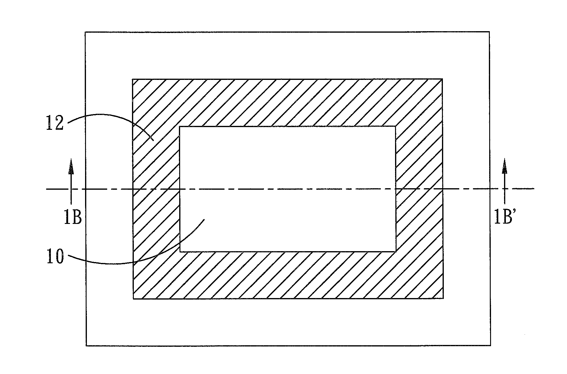
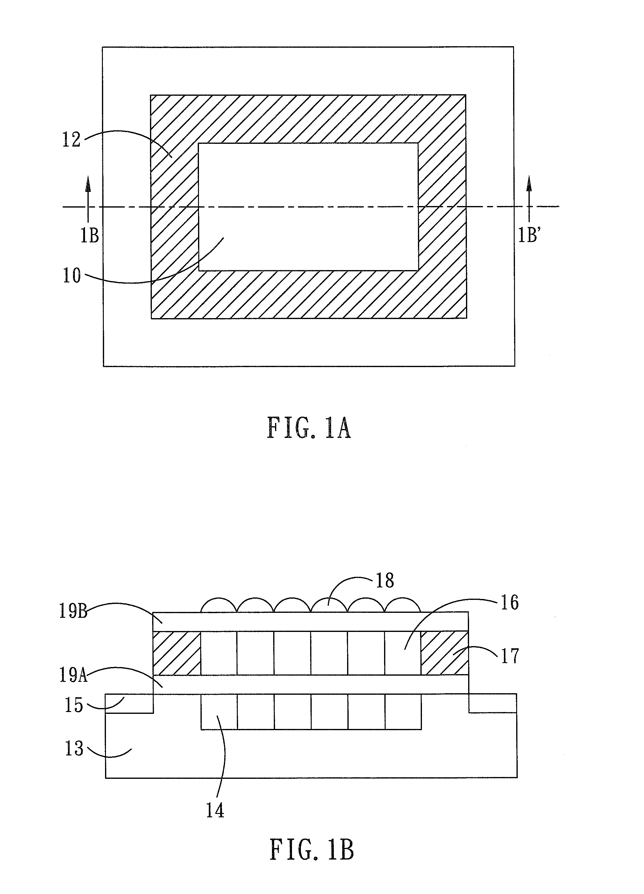
[0015]FIG. 1A shows a plan view of a complementary metal-oxide-semiconductor (CMOS) image sensor (or CIS) according to one embodiment of the present invention. FIG. 1B shows a cross-sectional view of the FIG. 1A CMOS image sensor along section line 1B-1B′. While the CMOS image sensor is illustrated in this embodiment, it is appreciated by those skilled in the pertinent art that the present invention may be well adapted to other visual input devices.
[0016]According to the plan view (FIG. 1A), the CMOS image sensor has, but is not necessarily limited to, a rectangular shape. The inner (rectangular) area of the CMOS image sensor is the active area (AA) 10 for performing visual input task (the image sensing in this case), and is usually known as the sensor area. The area surrounding the sensor area 10 in the peripheral area of the CMOS image sensor is the non-active area (NAA) 12, and is usually known as the non-sensor area. In the embodiment, the edge of the non-sensor area 12 is dista...
PUM
 Abstract
Description
Claims
Application Information
 - R&D
- Intellectual Property
- Life Sciences
- Materials
- Tech Scout
- Unparalleled Data Quality
- Higher Quality Content
- 60% Fewer Hallucinations
Browse by: Latest US Patents, China's latest patents, Technical Efficacy Thesaurus, Application Domain, Technology Topic, Popular Technical Reports.
© 2025 PatSnap. All rights reserved.Legal|Privacy policy|Modern Slavery Act Transparency Statement|Sitemap|About US| Contact US: help@patsnap.com


