
Bandgap circuit having a zero temperature coefficient

Inactive Publication Date: 2011-01-20
AICESTAR TECH SUZHOU CORP
View PDF5 Cites 20 Cited by
  • Summary
  • Abstract
  • Description
  • Claims
  • Application Information

AI Technical Summary

Benefits of technology

[0011]The present invention is directed to a bandgap circuit, which can normally work under an environment of a high threshold voltage and a low supply voltage, and can provide a stable bandgap reference voltage that is not influenced by temperature variation, so that an adverse effect caused by unmatched fabrication process can be mitigated.
[0017]The aforementioned bandgap circuit uses the single current path to promote the first input voltage and the second input voltage, so that the bandgap circuit can normally work under an environment of a high threshold voltage and a low supply voltage, and can provide a stable bandgap reference voltage that is not influenced by temperature variation. Since the single current path is used, unmatched problem of two resistors of the related art can be avoided, so that an adverse effect caused by unmatched fabrication process can be mitigated.

Problems solved by technology

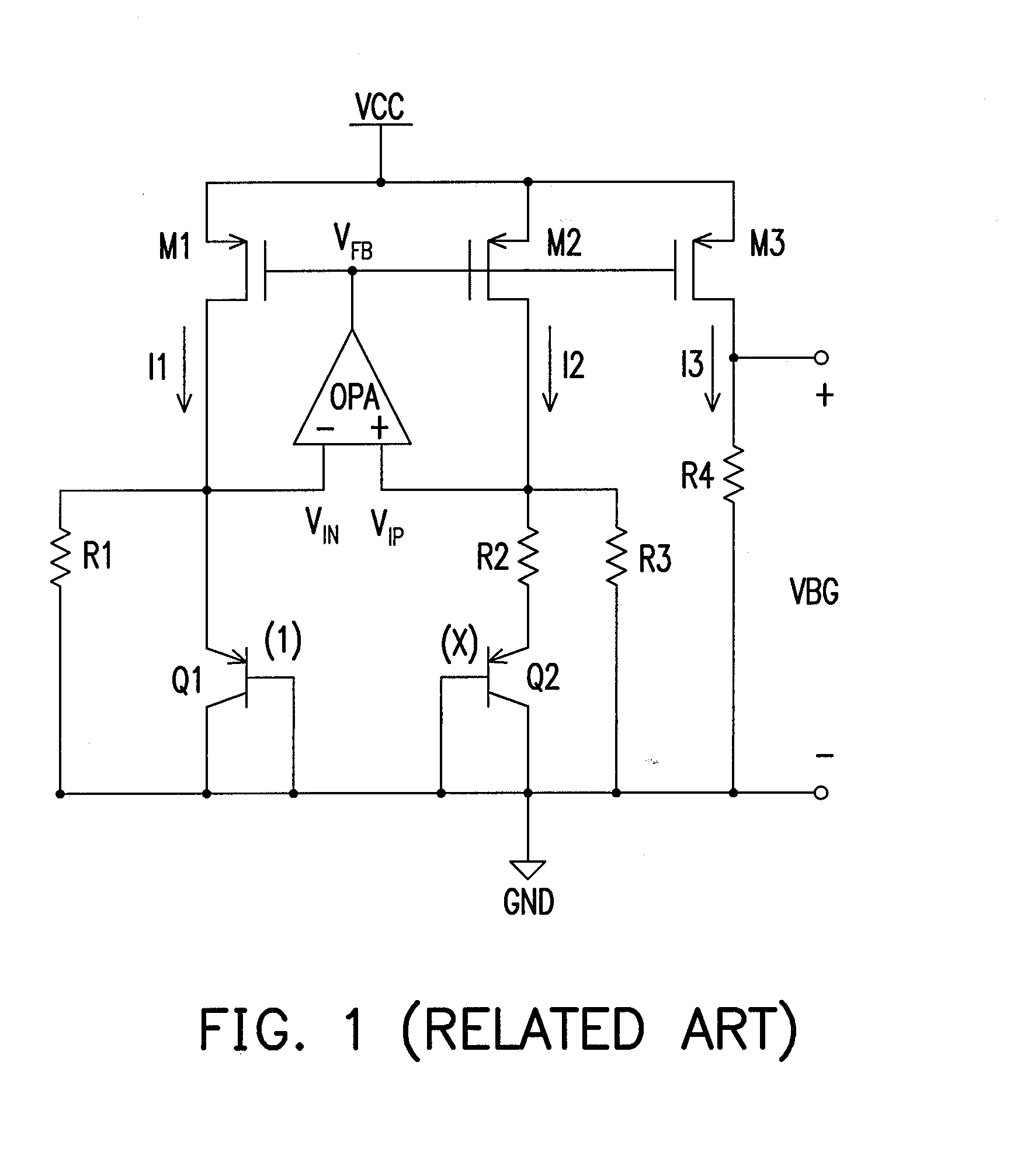
A problem is that if the threshold voltage VTHN is too high, within a system temperature range, the threshold voltage VTHN is probably greater than the input voltage VEB1 throughout, so that the operation amplifier OPA is unable to work.
If the threshold voltage |VTHP| is too high, within the system temperature range, VEB1+|VTHP| is probably greater than the supply voltage VCC throughout, so that the operation amplifier OPA is unable to work.
However, since variation of the fabrication process cannot be totally controlled, the PMOS transistors M1 and M2 of the current mirror are probably not totally matched, so that the current I1 is slightly different to the current I2, and the resistors R5 and R6 are probably not totally matched.
The above unmatched problem can result in a difference between the two input voltages VIN and VIP of the operation amplifier OPA, which may bring an adverse effect to the bandgap reference voltage VBG.

Method used


Image

  • Bandgap circuit having a zero temperature coefficient
  • Bandgap circuit having a zero temperature coefficient
  • Bandgap circuit having a zero temperature coefficient

Examples


Embodiment Construction

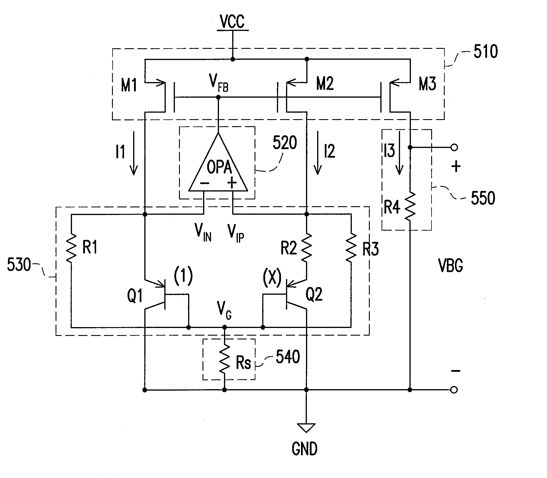
[0025]FIG. 5 is a schematic diagram illustrating a bandgap circuit according to an embodiment of the present invention. The bandgap circuit of FIG. 5 includes a current source 510, a voltage equalizer circuit 520, a voltage input circuit 530, a voltage boost circuit 540, and a voltage output circuit 550. The current source 510 provides three currents I1, I2 and I3, and maintains values of the three currents to a fixed ratio. For example, the currents I1, I2 and I3 can be equal, namely, I1:I2:I3=1:1:1. The voltage boost circuit 540 provides a boost voltage VG by a single current path. The voltage input circuit 530 is coupled to the voltage boost circuit 540, the voltage equalizer circuit 520, and the current source 510. The voltage input circuit 530 receives the currents I1 and I2, and provides input voltages VIN and VIP based on the boost voltage VG. The voltage equalizer circuit 520 is coupled to the current source 510 and the voltage input circuit 530, and receives the input volta...


PUM


Abstract

A bandgap circuit is provided, which includes a current source, a voltage boost circuit, a voltage input circuit, a voltage equalizer circuit, and a voltage output circuit. The current source provides a first current, a second current, and a third current, which are equal to one another. The voltage boost circuit provides a boost voltage by a single current path. The voltage input circuit receives the first and the second currents, and provides a first input voltage and a second input voltage based on the boost voltage. The voltage equalizer circuit receives the first and the second input voltages and equalize the two input voltages. The voltage output circuit provides a bandgap reference voltage according to the third current.

Description

BACKGROUND OF THE INVENTION[0001]1. Field of the Invention[0002]The present invention relates to a bandgap circuit. More particularly, the present invention relates to a bandgap circuit of a current mode and a voltage mode.[0003]2. Description of Related Art[0004]A bandgap circuit is used for generating a stable reference voltage that is not influenced by temperature variation. FIG. 1 is a circuit diagram illustrating a conventional current mode bandgap circuit. In which, metal oxide semiconductor field effect transistors (MOS transistors) M1, M2 and M3 form a current mirror to equalize currents I1, I2 and I3. Two input terminals of an operation amplifier OPA respectively receive input voltages VIN and VIP, and the input voltages VIN and VIP can be equalized by a virtual short circuit effect of the operation amplifier OPA. Resistors R1 and R3 have a same resistance, and the input voltages VIN and VIP are equal, so that currents flowing through the resistors R1 and R3 are the same, a...

Claims


Application Information

Patent Timeline
IPC IPC(8): G05F3/16
CPCG05F3/30
Inventor WANG, LING
Owner AICESTAR TECH SUZHOU CORP
Learn More