
Display device and drive method for the same

a technology of a display device and a drive method, which is applied in the field of display devices, can solve the problems of unsatisfactory display quality, and achieve the effects of stable voltage, reduced amplitude of video signals, and redistribution of charge amounts

Inactive Publication Date: 2010-12-09
SHARP KK
View PDF4 Cites 7 Cited by
  • Summary
  • Abstract
  • Description
  • Claims
  • Application Information

AI Technical Summary

Benefits of technology

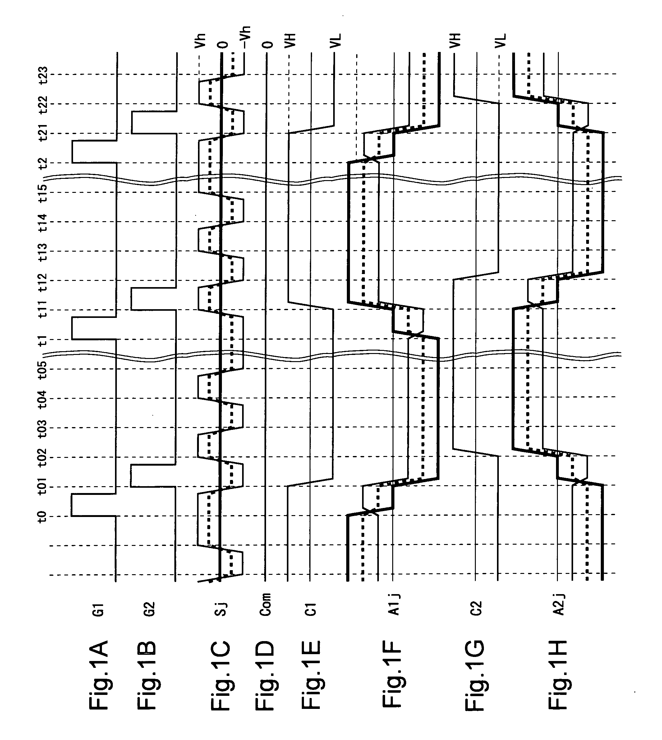
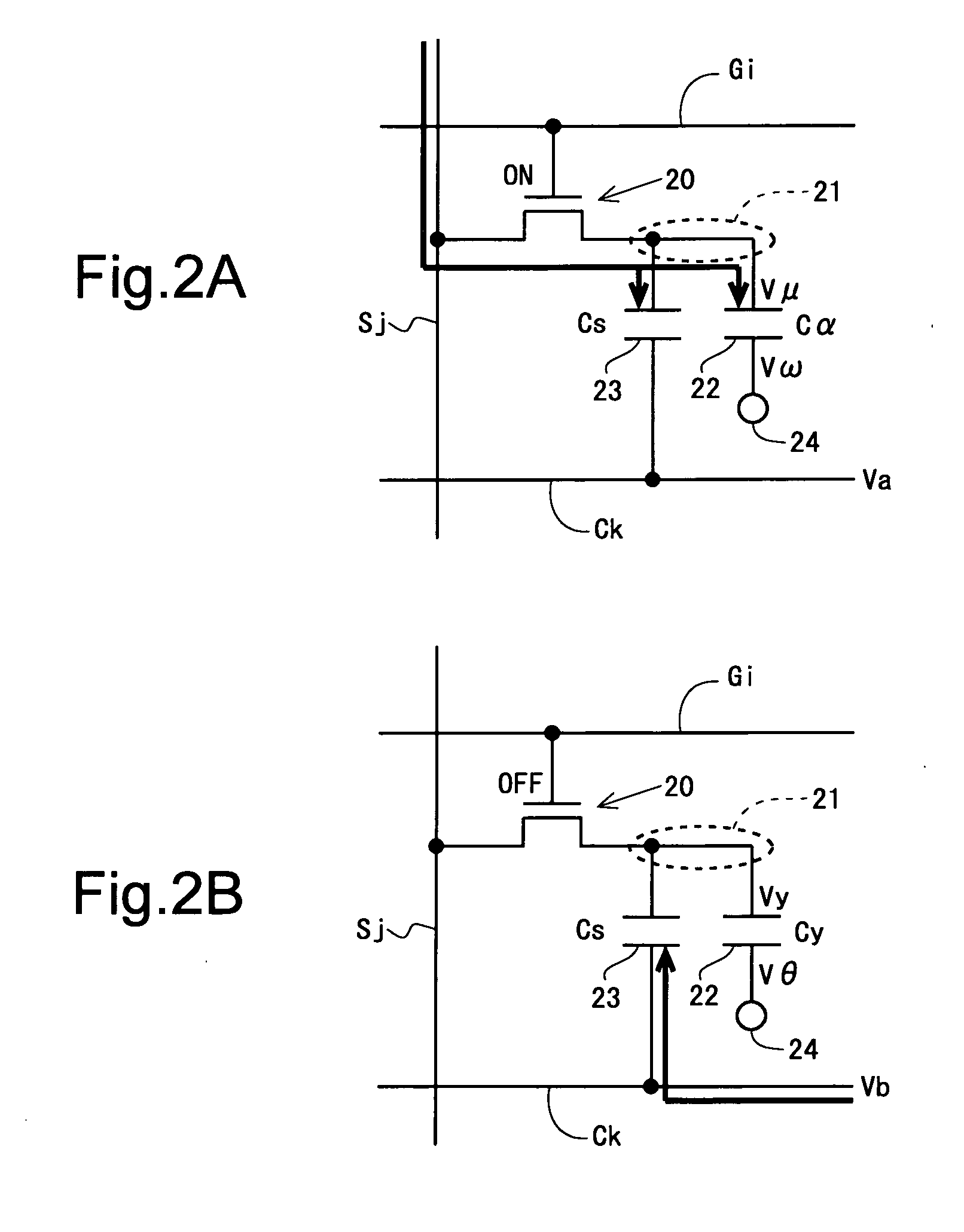
[0057]The following effects can be achieved by the first aspect of the present invention. Note that it is assumed here that a target voltage to be applied to the element capacitance is Vβ, a voltage applied to the pixel electrode during the first period is Vμ, a voltage applied to the auxiliary capacitance line during the first period is Va, a voltage applied to the auxiliary capacitance line during the second period is Vb, an element capacitance value during the first period is Cα, and an element capacitance value corresponding to the target voltage Vβ is Cβ. In a frame period in which the target voltage Vβ of one polarity is to be applied to the element capacitance, during the first period, the voltage Vβ of the other polarity based on the target voltage Vβ is applied to the pixel electrode, and during the second period, the voltage on the auxiliary capacitance line changes from the voltage Va of the other polarity to the voltage Vb of one polarity. Here, the voltage Vμ can be set such that the voltage applied to the element capacitance is Vβ during the second period when the element capacitance value is in steady state at Cβ through the first and second periods. By setting the voltage Vμ in such a manner, a charge Cα×Vμ provided to the element capacitance during the first period becomes lower than Cβ×Vβ (in absolute value) when the element capacitance value Cα during the first period is lower than Cβ. The voltage Vμ is opposite in polarity to the target voltage Vβ, and therefore the voltage applied to the element capacitance during the second period becomes higher than the target voltage Vβ as the charge provided to the element capacitance during the first period decreases. Accordingly, when a transition state is such that the element capacitance value changes from low value to high value, a voltage above the target voltage Vβ is applied to the element capacitance. On the other hand, when the element capacitance value Cα during the first period is higher than Cβ, the charge Cα×Vμ provided to the element capacitance during the first period becomes higher than Cβ×Vβ (in absolute value). The voltage Vμ is opposite in polarity to the target voltage Vβ, and therefore the voltage applied to the element capacitance during the second period becomes lower than the target voltage Vβ as the charge provided to the element capacitance during the first period increases. Accordingly, when the transition state is such that the element capacitance value changes from high value to low value, a voltage below the target voltage Vβ is applied to the element capacitance.
[0058]According to the second aspect of the present invention, positive-polarity voltage and negative-polarity voltage are alternatingly applied to the common electrode. As a result, the amplitude of a video signal can be reduced when compared to a configuration in which a constant voltage is applied to the common electrode.
[0059]According to the third aspect of the present invention, during the second period, the potential of the auxiliary capacitance line changes in accordance with the change of the potential of the common electrode. As a result, the amount of charge redistributed between the auxiliary capacitance and the element capacitance decreases, and therefore a stable voltage is applied to the element capacitance.
[0060]According to the fourth aspect of the present invention, the auxiliary capacitance line is brought into an electrically floating state during the second period. Here, the pixel electrode and the common electrode are capacitively coupled, and the pixel electrode and the auxiliary capacitance line are capacitively coupled. Accordingly, during the second period, the potential of the auxiliary capacitance line changes in accordance with the change of the potential of the common electrode. As a result, a stable voltage is applied to the element capacitance, as in the third aspect of the present invention.
[0061]According to the fifth aspect of the present invention, it is ensured that the second period is ensured to be long enough to apply the target voltage to the element capacitance.
[0062]According to the sixth aspect of the present invention, for the auxiliary capacitance lines, a plurality of them are driven at a time, and therefore the scale of the circuit for driving the auxiliary capacitance lines can be reduced.

Problems solved by technology

As a result, when a display is provided such that images change every frame, satisfactory display quality is not obtained.

Method used


Image

  • Display device and drive method for the same
  • Display device and drive method for the same
  • Display device and drive method for the same

Examples


first embodiment

2. First Embodiment

2.1 Overall Configuration and Operation

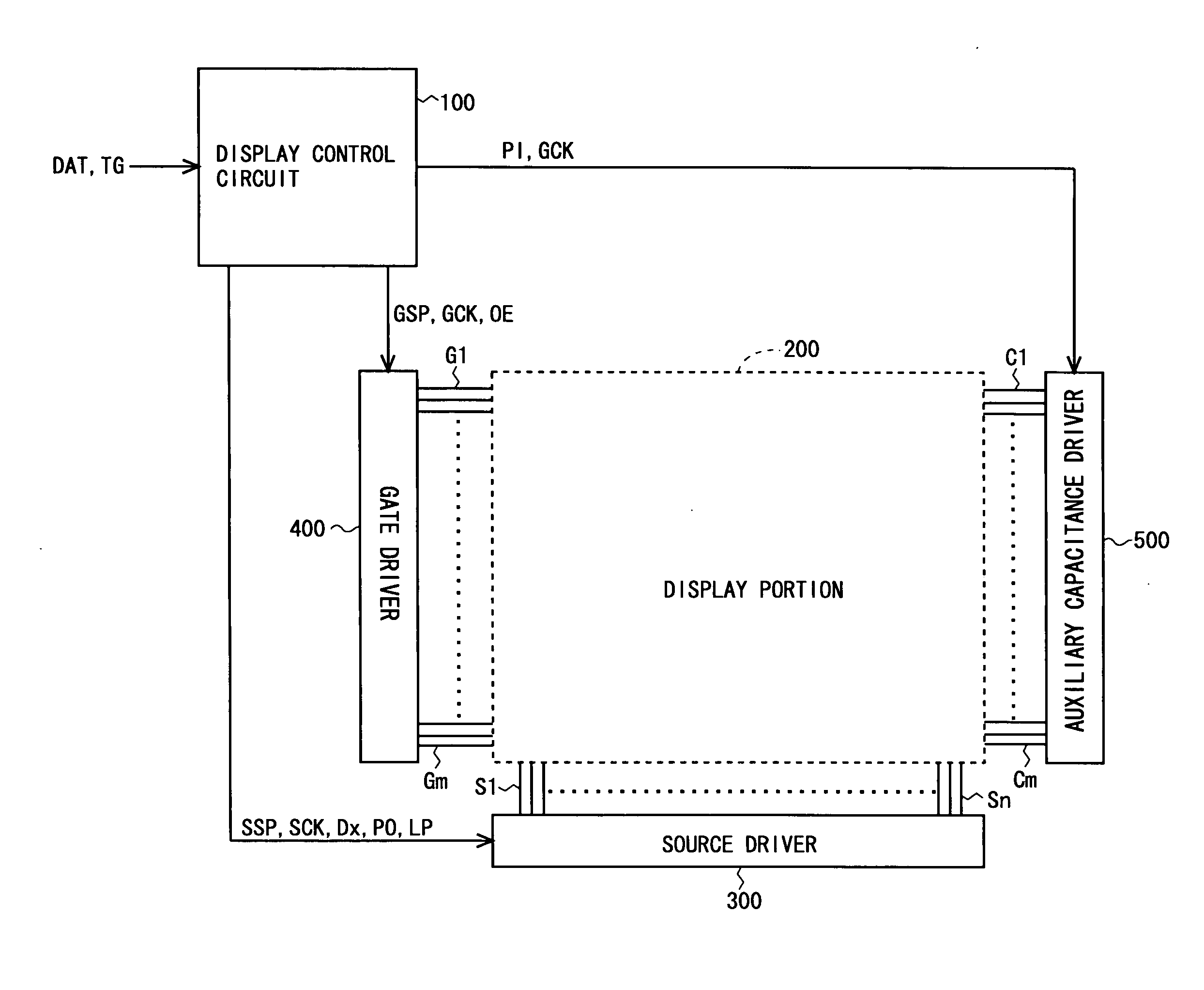
[0130]FIG. 6 is a block diagram illustrating the overall configuration of a liquid crystal display device according to a first embodiment of the present invention. The liquid crystal display device includes a display control circuit 100, a display portion 200, a source driver (video signal line driver circuit) 300, a gate driver (scanning signal line driver circuit) 400, and an auxiliary capacitance driver (auxiliary capacitance electrode driver circuit) 500. In the following descriptions, the source driver 300, the gate driver 400, and the auxiliary capacitance driver 500 are also collectively referred to as drivers (driver circuits). FIG. 7 is a block diagram illustrating detailed configurations of the drivers and the display portion 200 in the liquid crystal display device. Note that descriptions will be provided on the assumption that a 256 gray-scale gradation display is performed in the liquid crystal display device.

[01...

second embodiment

3. Second Embodiment

3.1 Configuration

[0164]FIG. 10 is a block diagram illustrating detailed configurations of drivers and a display portion 200 in a liquid crystal display device according to a second embodiment of the present invention. In the present embodiment, an opposing electrode driver 600 for driving an opposing electrode 24 is provided, along with components in the first embodiment. Also, the source output circuit in the source driver is configured differently from that of the first embodiment. Other components are the same as those of the first embodiment, and therefore any descriptions thereof will be omitted.

[0165]The opposing electrode driver 600 is provided with an opposing electrode polarity signal PC from the display control circuit 100. The opposing electrode driver 600 drives the opposing electrode 24 based on the opposing electrode polarity signal PC. Specifically, the opposing electrode driver 600 provides the opposing electrode 24 with a voltage of 0V alternatin...

third embodiment

4. Third Embodiment

4.1 Configuration

[0184]In a liquid crystal display device according to the present embodiment, general configurations of the drivers and the display portion 200 are the same as in the second embodiment shown in FIG. 10. However, there are differences from the second embodiment in terms of the magnitude of a voltage provided to the auxiliary capacitance lines C1 to Cm from the auxiliary capacitance driver 500 and the magnitude of a voltage provided to the opposing electrode 24 from the opposing electrode driver 600. Specifically, while in the second embodiment, the first-period opposing electrode voltage Vω is set to be equal in magnitude to the source voltage having a gray-scale value of “255” (a voltage of 0V or the source high voltage Vh), in the present embodiment, the first-period opposing electrode voltage Vω is set to be “−Vd” on the low-potential side and “Vh+Vd” on the high-potential side. In this manner, in the present embodiment, the amplitude of the opp...


PUM


Abstract

At least one embodiment of the present invention aims to provide a display device capable of compensating for a change of a liquid crystal capacitance value for an electro-optic element such as a liquid crystal in accordance with a change of an application voltage to the electro-optic element, without incorporating frame memory. It also aims to improve the response speed of a display device without frame memory. For each pixel formation portion, a frame period is divided into first and second periods. During a frame period in which a target voltage having one of the positive and negative polarities with respect to a potential (Com) of an opposing electrode is to be applied to a pixel electrode, during the first period, a TFT is brought into conductive state and a voltage corresponding to the target voltage is applied to a source line (Sj), thereby providing the pixel electrode with a voltage of the other polarity with respect to the potential (Com) of the opposing electrode, while during the second period, the TFT is brought into non-conductive state and the voltage on an auxiliary capacitance line (Ck) is caused to change from the other polarity to one polarity with respect to the potential of the opposing electrode.

Description

TECHNICAL FIELD[0001]The present invention relates to display devices such as liquid crystal display devices and drive methods for the same.BACKGROUND ART[0002]In recent years, liquid crystal display devices for notebook computers, cell phones, liquid crystal televisions, etc., which use TFTs (Thin Film Transistors), have come into wide use. In a liquid crystal display device using TFTs, to control the state of display by a liquid crystal, a driver circuit called a “source driver” supplies voltage to the liquid crystal. For example, Japanese Laid-Open Patent Publication No. 2002-351409 discloses an invention of a liquid crystal display device having a configuration shown in FIG. 18. This liquid crystal display device is provided with a source driver 907 consisting of a plurality of source driver ICs 908, which supplies voltage to a liquid crystal.[0003]FIG. 8 is a circuit diagram illustrating the configuration of a pixel formation portion in a typical liquid crystal display device. ...

Claims


Application Information

Patent Timeline
Patent Type & Authority Applications(United States)
IPC IPC(8): H04N3/14
CPCG09G3/3614G09G3/3655G09G2320/0252G09G2310/08G09G2300/0876
Inventor NUMAO, TAKAJITERANUMA, OSAMU
Owner SHARP KK
Learn More