Method for manufacturing nonvolatile storage device
- Summary
- Abstract
- Description
- Claims
- Application Information
AI Technical Summary
Benefits of technology
Problems solved by technology
Method used
Image

Examples
first embodiment
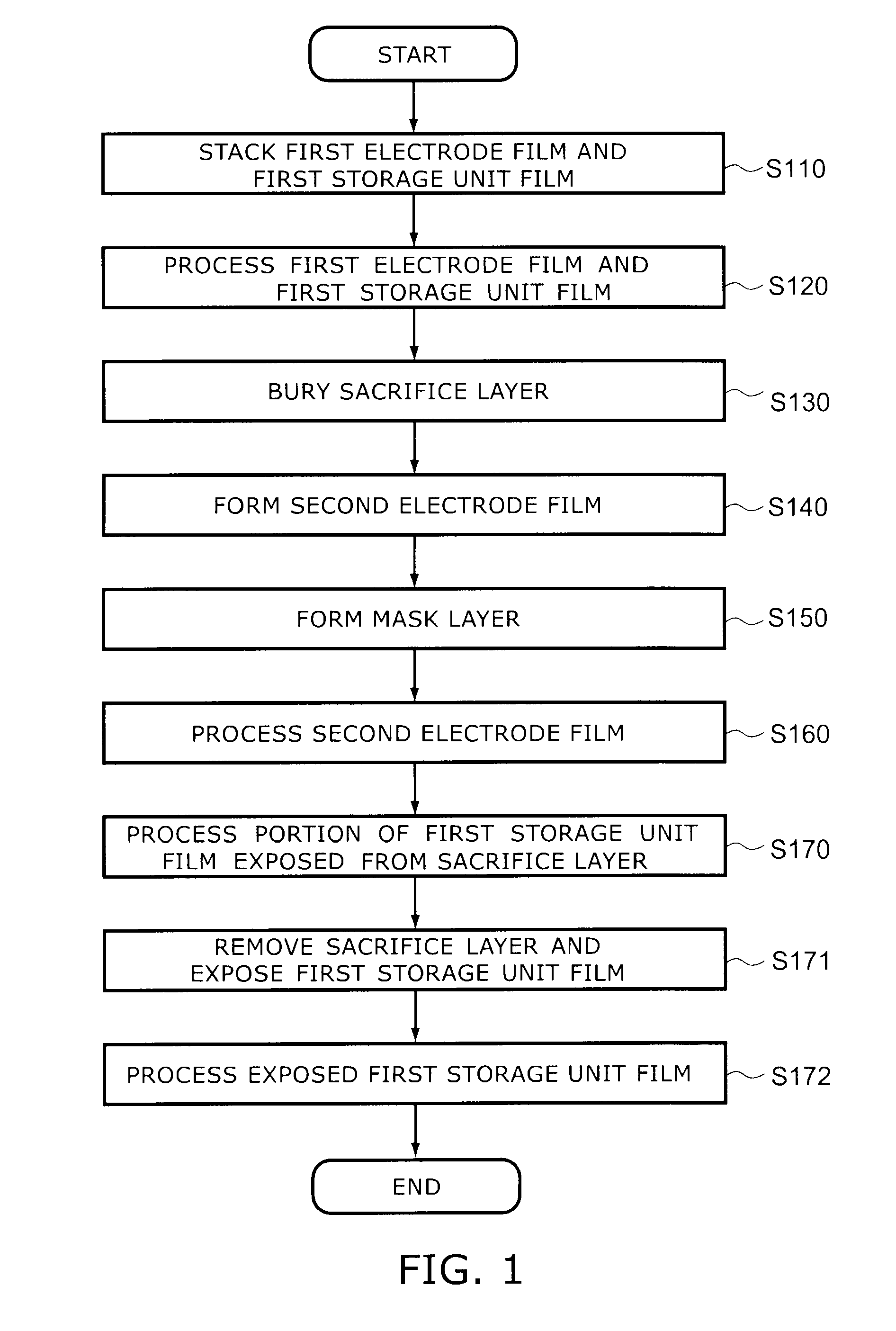
[0057]FIG. 1 is a flow chart illustrating a method for manufacturing a nonvolatile storage device according to a first embodiment of the invention.
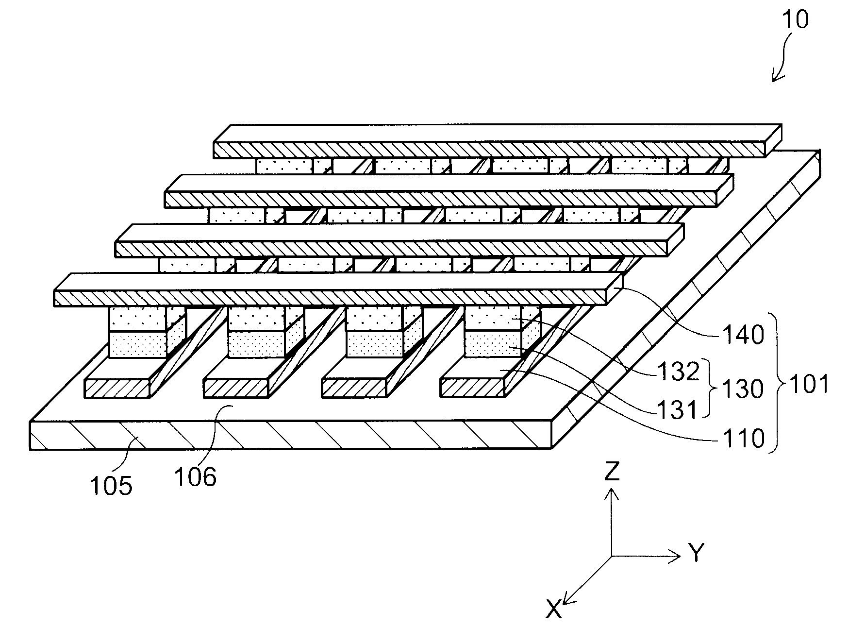
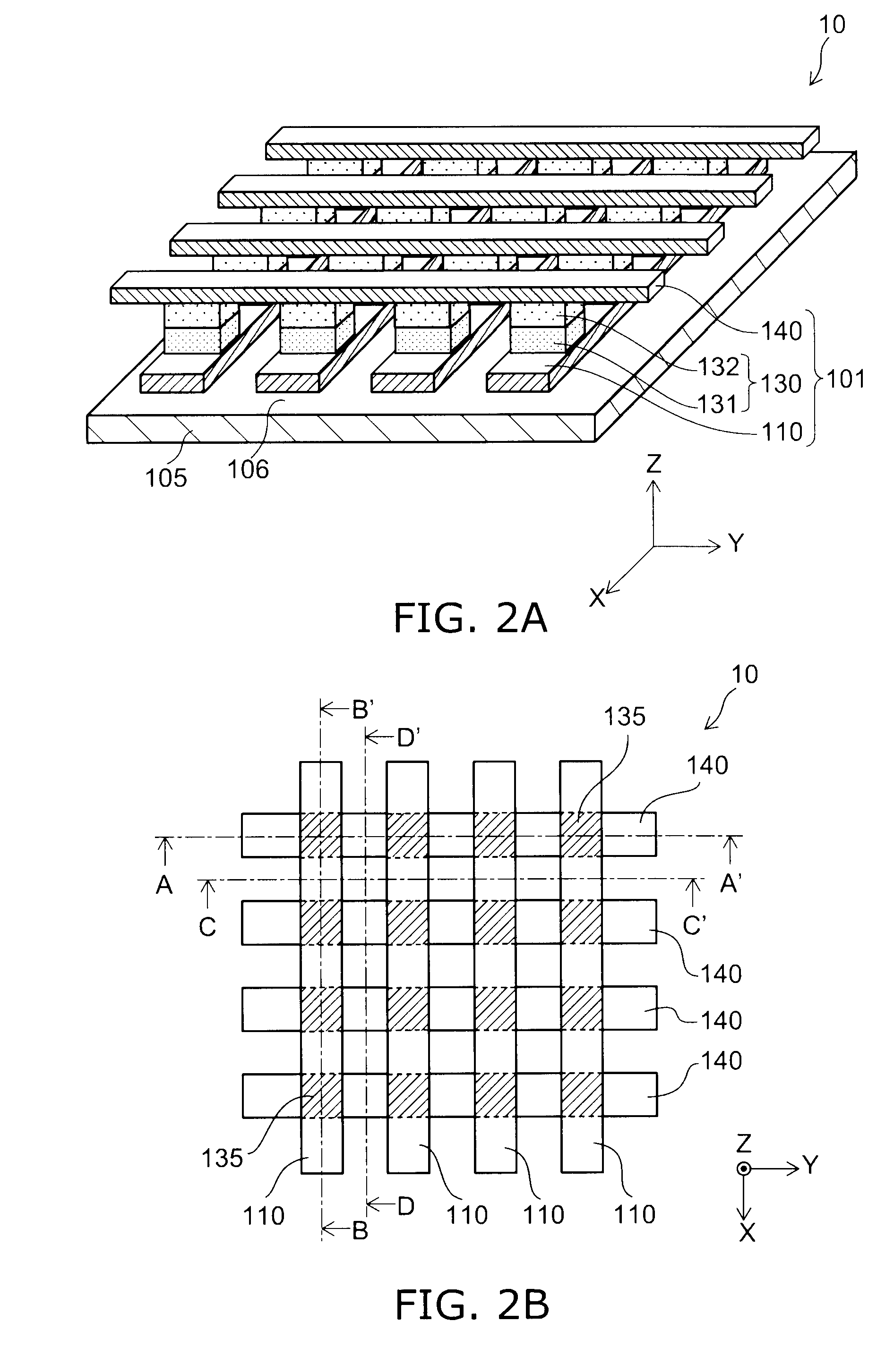
[0058]FIGS. 2A and 2B are schematic views illustrating the configuration of a nonvolatile storage device manufactured by the method for manufacturing a nonvolatile storage device according to the first embodiment of the invention.
[0059]Specifically, FIG. 2A is a perspective view, and FIG. 2B is a plan view.
[0060]FIGS. 3A to 3D are schematic cross-sectional views illustrating the configuration of the nonvolatile storage device manufactured by the method for manufacturing a nonvolatile storage device according to the first embodiment of the invention.
[0061]Specifically, FIG. 3A is a cross-sectional view taken along line A-A′ of FIG. 2B, FIG. 3B is a cross-sectional view taken along line B-B′ of FIG. 2B, FIG. 3C is a cross-sectional view taken along line C-C′ of FIG. 2B, and FIG. 3D is a cross-sectional view taken along line D-D′ of FIG. 2B....
second embodiment
[0147]A method for manufacturing a nonvolatile storage device according to a second embodiment of the invention is used for a nonvolatile storage device in which a plurality of memory cell arrays are stacked.
[0148]FIG. 14 is a flow chart illustrating a method for manufacturing a nonvolatile storage device according to the second embodiment of the invention.
[0149]FIGS. 15A and 15B are schematic views illustrating the configuration of a nonvolatile storage device manufactured by the method for manufacturing a nonvolatile storage device according to the second embodiment of the invention.
[0150]Specifically, FIG. 15A is a perspective view, and FIG. 15B is a plan view.
[0151]FIGS. 16A to 16D are schematic cross-sectional views illustrating the configuration of the nonvolatile storage device manufactured by the method for manufacturing a nonvolatile storage device according to the second embodiment of the invention.
[0152]Specifically, FIG. 16A is a cross-sectional view taken along line A-A...
third embodiment
[0185]FIG. 20 is a flow chart illustrating a method for manufacturing a nonvolatile storage device according to a third embodiment of the invention.
[0186]FIGS. 21A and 21B are schematic views illustrating the configuration of a nonvolatile storage device manufactured by the method for manufacturing a nonvolatile storage device according to the third embodiment of the invention.
[0187]Specifically, FIG. 21A is a perspective view, and FIG. 21B is a plan view.
[0188]FIGS. 22A to 22D are schematic cross-sectional views illustrating the configuration of the nonvolatile storage device manufactured by the method for manufacturing a nonvolatile storage device according to the third embodiment of the invention.
[0189]Specifically, FIG. 22A is a cross-sectional view taken along line A-A′ of FIG. 21B, FIG. 22B is a cross-sectional view taken along line B-B′ of FIG. 21B, FIG. 22C is a cross-sectional view taken along line C-C of FIG. 21B, and FIG. 22D is a cross-sectional view taken along line D-D...
PUM
 Abstract
Description
Claims
Application Information
 - R&D
- Intellectual Property
- Life Sciences
- Materials
- Tech Scout
- Unparalleled Data Quality
- Higher Quality Content
- 60% Fewer Hallucinations
Browse by: Latest US Patents, China's latest patents, Technical Efficacy Thesaurus, Application Domain, Technology Topic, Popular Technical Reports.
© 2025 PatSnap. All rights reserved.Legal|Privacy policy|Modern Slavery Act Transparency Statement|Sitemap|About US| Contact US: help@patsnap.com